Download
1 / 29
290 likes | 324 Vues
Learn the NMOS physical structure and the I-V characteristics for MOS transistors. Explore transistor geometry, capacitance, scaling, and electrical model. Understand the behavior of NMOS and PMOS transistors in saturation and linear regions. Gain insights into transistor switching, effective resistance, and circuit modeling in digital systems.

E N D
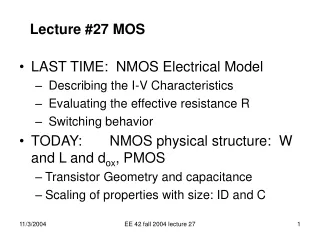
Lecture #27 MOS • LAST TIME: NMOS Electrical Model • Describing the I-V Characteristics • Evaluating the effective resistance R • Switching behavior • TODAY: NMOS physical structure: W and L and dox, PMOS • Transistor Geometry and capacitance • Scaling of properties with size: ID and C EE 42 fall 2004 lecture 27
We have an equation for ID in the saturation region. ID ID IDS ID for VGS = maximum (VDD) D If VGS = 0. VDS D G VDD RDN G S Electrical Model S NMOS as a Switch - Summary N Ch The circuit symbol The value of RDN is chosen to predict the correct timing delay. Then we can essentially replace the transistor with the simple switch model (valid of course only for predicting timing delays). EE 42 fall 2004 lecture 27
ID = IDSX (1+ l VDS) ID VGS = VDD G S D (-1/lis intercept with VDS axis) l IDSis slope iD + VGS VDS + - IDS is the intercept with ID axis VDS MOS “Theory” For simple digital circuit calculations the MOS transistor will be essentially off (VGS < VT ) or fully turned on (VGS = VDD ), the power supply voltage). In the saturation region we describe the variation of ID with VDS with the empirical equation : on IDS off Then we can estimate the effective resistance in terms of l and IDS EE 42 fall 2004 lecture 27
G D + - + C VOUT - S Thus the average effective resistance is the ratio: (3/4) VDD /IDS( 1+lX(3/4)VDD) =RDN slope = 1/RDN The effective resistance with VGS = VDD The MOS transistor discharges C. (VDD to VDD /2) As VOUT goes from VDD to VDD /2, the average voltage VDS is (3/4) VDD. Since ID = IDS( 1+lXVDS) The average current is IDS( 1+lX(3/4)VDD) . VIN =3V - ID VGS = VDD Using a resistance of this value we get discharge time estimate which is less than 4% different from the correct answer obtained by direct integration IDS VGS = 0 VDS VDD VDD/2 EE 42 fall 2004 lecture 27
ID ID = IDSX (1+ l VDS) on VGS = VDD IDS G S D iD + VGS VDS + - VDS off But if VGS = VDD the value of IDS depends on VGS, so we need some more theory. In particular we want to: • Describe dependence of IDS on VGS and geometry • Describe the “break point” in VDS above which ID saturates. MOS I-V Characteristics in more detail For simple digital circuit calculations the MOS transistor will be essentially off (VGS < VT ) or fully turned on (VGS = VDD ), the power supply voltage). EE 42 fall 2004 lecture 27
We call the boundary between the regions VDSat. ID VGS G S D iD + VGS VDS + - VDS VDSat A little more MOS “Theory” We have two regions: the resistive region at smaller VDS and the saturation region at higher VDS . In the resistive region we start out like a simple resistor between source and drain (whose value depends on gate voltage) and gradually the curve “bends over” as we approach saturation In the saturation we have a small gradual increase of I with VDS Now we wish to describe the dependence of the current on VGS EE 42 fall 2004 lecture 27
n n - + gate oxide insulator drain source P Below threshold VGS < Vt Below threshold, there are no electrons under the gate oxide, and the holes in the substrate are blocked from carrying current by reverse biased diode junctions EE 42 fall 2004 lecture 27
n n VGS > Vt - + gate oxide insulator drain source P NMOS in the linear (Triode) region If the gate voltage is above threshold, but the source to drain voltage is small, the charge under the gate is uniform, and carries current much like a resistor The electrons move under the influence of the Electric field at a velocity: ν=μE where E=volts/distance And they must travel a distance L to cross the gate Since the total charge is Q=CVgs, we will have a current Id=μCgateVds (Vgs-Vth)/L2= μ(εox/dox)Vds (Vgs-Vth)W/L EE 42 fall 2004 lecture 27
n n - + gate oxide insulator drain source P NMOS with increasing Vds VGS > Vt As the voltage from the source to the drain is increased, the current increases, but not by as much because the charge is attracted out from under the oxide, beginning to pinch off the channel EE 42 fall 2004 lecture 27
Saturation • As the Source-Drain voltage is increased, there will be a significant change in the charge at different distances along the gate • When the voltage across the device at the drain end goes below threshold, the current is pinched off. • If there is no current out the drain end, however, the current due to the carriers which are available from the source cause the voltage to be closer to that of the source. • These two effects cause a small region to form near the drain which limits the current. This is called saturation EE 42 fall 2004 lecture 27
n n - + gate oxide insulator drain source P NMOS in saturation VGS > Vt When the voltage from the source to the drain gets high enough, the channel gets “pinched” In the pinch region, the carriers move very fast, but the current is determined by the triangular region, which does not change much as the drain voltage is changed, so the current saturates EE 42 fall 2004 lecture 27
Submicron MOS • In the last few years, transistors have become so small that some of these approximations are breaking down: • As the transistors get short, the difference between the triode region and saturation has become blurred, with no clear saturation • Because gate oxides are so thin, some current goes through the gate in a process called tunneling • Sub-Threshold currents are increasing, causing the transistors to conduct a small amount even when they are supposed to be off. EE 42 fall 2004 lecture 27
ID VGS VGS = 4 VGS = 3 VGS = 2 VDS 1/l VDSat MOS “Theory”, con’t In the saturation region (VDS >VDSat ) all the curves are described by ID = IDSX (1+ l VDS) but IDS is a function of VGS. In modern devices the saturation current is proportional to (VGS-VT). The simple field effect gives us the idea for this proportionality: As we increase VGS there is some “threshold”, VT. above which electrons accumulate on the surface. The current is of course proportional to the number of these electrons, so it is proportional to (VGS -VT). In figure below VT = 1V. Note that the current is proportional to (VGS -VT), for example the current at VGS=3V is double that at VGS =2V. The intercepts with the current axis (IDS) depends not only on the gate voltage, but also on device geometry. We will next discuss how IDS depends on device geometry. EE 42 fall 2004 lecture 27
W L n n Contact to Drain Contact to Source “Metal” gate (Al or Si) gate P-type Silicon oxide insulator NMOS TRANSISTOR STRUCTURE NMOS = N-channel Metal Oxide Silicon Transistor EE 42 fall 2004 lecture 27
gate length • The gate length, L, is the distance the electrons have to travel. It is generally set at the minimum value (eg .18 micron) for nearly all logic transistors • As the gate length gets shorter, the gate capacitance gets smaller • As the gate length gets shorter, the current drive of the transistor also gets larger. • However, leakage current also increases EE 42 fall 2004 lecture 27
Gate width • The gate width, W, is determined by the circuit designer. One uses a wider gate to get more current (and thus charge a capacitor faster). For example doubling W is the same as putting two equal-sized transistors in parallel, and thus doubles the current at any given voltage. EE 42 fall 2004 lecture 27
n n “Metal” gate (Al or Si) gate P-type Silicon oxide insulator NMOS TRANSISTOR CAPACITANCE W L Contact to Drain Contact to Source dOX = oxide thickness The gate is insulated from the rest of the transistors, but it has a substantial capacitance to the source as it builds up charge in the channel The capacitance is proportional to W and L (for logic, mostly L is fixed, so in effect C is proportional to the gate width W that the designer chooses. It is inversely proportional to dOX . EE 42 fall 2004 lecture 27
W L Thin oxide MOS TRANSISTOR – TOP VIEW What are device dimensions? Gate Length = L and is fixed for any technology. (Such as the .09-0.18 mm technology in manufacturing today). Drain contact Gate (over oxide) Gate Width = W and is selected by the circuit designer for the current required. Source contact The device current is proportional to W as well as (VGS -VT), so we express IDS as a constant times ( IDS' ) times W times (VGS -VT). (Thusthe units of the constant IDS' are mA/V-mm.) We multiply IDS' by the gate width W and by (VGS -VT). to get the value of IDS inmA. ID = IDSX (1+ l VDS) and IDS = W X IDS' (VGS -VT). Example: a “1/4mm device” with IDS' = 75 mA/V-mm , W = 5mm, l= 0.02 V-1, VT = 0.5V and in a circuit with VDD = 2.5V. If the device were 5mm wide and the gate were at VDD then IDS = 5 X 75 (2.5 -0.5) = 750mA. EE 42 fall 2004 lecture 27
Drain contact W L Gate (over oxide) Source contact MOS TRANSISTOR – TOP VIEW Gate Capacitance: The dimensions of the capacitor are area = W X L and thickness = dOX . A typical value, say for “1/4 mm” technology, is 5nm. The capacitance formula from physics is C=εA/d = W X L X eOX / dOX. The dielectric constant for oxide, eOX, is 3.9 eO = 3.45X10⁻¹³ f/cm. If dOX = 5nm then eOX / dOX =7fF/mm2 of capacitor so C=7W X L (fF) with W and L in mm. Example: The same “1/4mm device” device with, W = 5mm. The gate capacitance is 5 X 0.25 X 7 fF = 8.6 fF. EE 42 fall 2004 lecture 27
VDD = 3V VIN =3V + VOUT RN This is what we use the NMOS for - VSS = 0V VOUT VDD = 3V - RP VIN =0V + VIN jumps from 0V to 3V VOUT t - - VSS = 0V Controlled Switch Model of Inverter (Lect. 18) If there is a capacitance at the output node (there always is) then VOUT responds to a change in VIN with our usual exponential form. Output when VIN jumps from 3V to 0V 3 0 EE 42 fall 2004 lecture 27
G D + - + C VOUT - S Purpose of the NMOS Switch The MOS transistor discharges C (some load). The NMOS switch is great for discharging a node to ground. When VIN goes high (VDD ) then VOUT goes from VDD to ground. When it reaches VDD /2 we call that time the stage delay. VIN =3V - ID VGS = VDD But we also need a switch to charge a node, i.e. bring it from ground up toward VDD . That’s where we need another type of transistor, the PMOS. It makes the ideal switch to charge the node. IDS VDS VDD VDD/2 EE 42 fall 2004 lecture 27
PMOS circuit symbol D D G G S S CIRCUIT SYMBOLS NMOS circuit symbol A small circle is drawn at the gate to remind us that the polarities are reversed for PMOS. EE 42 fall 2004 lecture 27
In this device the gate controls electron flow from source to drain. (in the absence of gate voltage, current is blocked) n n n n N-MOS source drain VGS > Vt P - + gate oxide insulator oxide insulator drain source P NMOS =device which carrier current using electrons but on the surface of a p-type substrate (p-type substrate means that no electrons are available) gate If we increase gate voltage to a value greater than Vt then a conducting channel forms between source and drain. (“Closed switch”) EE 42 fall 2004 lecture 27
In this device the gate controls electron flow from source to drain. n n N-MOS source drain P gate oxide insulator P-MOS drain source In this device the gate controls hole flow from source to drain. p p n-type Si CMOS = Complementary MOS(PMOS is a second Flavor) gate It is made in p-type silicon. The NEW FLAVOR!P-MOS It is made in n-type silicon. (In n-type silicon no positive charges (“holes”) are normally around.) EE 42 fall 2004 lecture 27
gate P-MOS drain source n-type Si |VGS |>|Vt | + - gate drain In this device the gate controls hole flow from source to drain. p p p p n-type Si source PMOS The body is n-type silicon. What if we apply a big negative voltage on the gate? If |VGS |>|Vt | (both negative) then we induce a + charge on the surface (holes) EE 42 fall 2004 lecture 27
p p G S D ID G n n p S D ID B n ID ID VGS=3V VGS= 3V B 1 mA 1 mA (for IDS = 1mA) (for IDS = -1mA) VGS=0 VGS=0 VDS VDS 2 4 1 3 2 4 1 3 NMOS and PMOS Compared NMOS “Body” – p-type Source – n-type Drain – n-type VGS – positive VT – positive VDS – positive ID – positive (into drain) PMOS “Body” – n-type Source – p-type Drain – p-type VGS – negative VT – negative VDS – negative ID – negative (into drain) EE 42 fall 2004 lecture 27
VDD VDD S S S VG =0 G G G VDD VG = VDD V=0 D D D Switch OPEN Switch CLOSED Switch is closed: Drain (D) is connected to Source (S) when VG =0 Switch is open : Drain (D) is disconnected from Source (S) when VG = VDD PMOS Transistor Switch Model Operation compared to NMOS: It is complementary. For PMOS for the normal circuit connection is to connect S to VDD (The function of the device is a “pull up”) EE 42 fall 2004 lecture 27
S CGS G S G RDP D D The Switch model PMOS Model Refinement PMOS transistor has an equivalent resistance RDPwhen closed There is also a gate capacitance CGS, just as in NMOS P Ch The circuit symbol EE 42 fall 2004 lecture 27
CMOS Challenge: build both NMOS and PMOS on a single silicon chip NMOS needs a p-type substrate PMOS needs an n-type substrate Requires extra process steps D G G D S S oxide P-Si n-well p p n n EE 42 fall 2004 lecture 27


