Programmable Logic Devices in Integrated Circuit Design
580 likes | 786 Vues
Learn about Programmable Logic Devices (PLDs), including types, structures, and programming methods. Understand the benefits of PLDs in complex digital logic designs and how they help in reducing PCB complexity.

Programmable Logic Devices in Integrated Circuit Design
E N D
Presentation Transcript
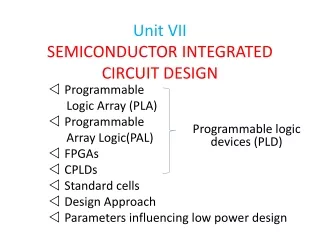
Unit VIISEMICONDUCTOR INTEGRATED CIRCUIT DESIGN Programmable logic devices (PLD) Programmable Logic Array (PLA) Programmable Array Logic(PAL) FPGAs CPLDs Standard cells Design Approach Parameters influencing low power design
PLD Programmable logic is defined as a device with configurable logic and flip-flops linked together with programmable interconnect. Why we are going for PLDs • Problems by Using Basic Gates • Many components on PCB: • As no. of components rise, nodes interconnection complexity grow exponentially • Growth in interconnection will cause increase in interference, PCB size, PCB design cost, and manufacturing time
PROGRAMMABLE LOGIC DEVICES (PLD) PLD Hierarchical Architecture
PLD • The purpose of a PLD device is to permit elaborate digital logic designs to be implemented by the user in a single device. • Can be erased electrically and reprogrammed with a new design, making them very well suited for academic and prototyping • Types of Programmable Logic Devices • SPLDs (Simple Programmable Logic Devices) • ROM (Read-Only Memory) • PLA (Programmable Logic Array) • PAL (Programmable Array Logic) • GAL (Generic Array Logic) • CPLD (Complex Programmable Logic Device) • FPGA (Field-Programmable Gate Array)
PLD • The first three varieties(ROM, PLA, PAL) are quite similar to each other: • They all have an input connection matrix, which connects the inputs of the device to an array of AND-gates. • They all have an output connection matrix, which connect the outputs of the AND-gates to the inputs of OR-gates which drive the outputs of the device. • The gate array is significantly different and will be described later.
PLD • The differences between the first three categories are these: • 1. In a ROM, the input connection matrix is hardwired. The user can modify the output connection matrix. • In a PAL/GAL the output connection matrix is hardwired. The user can modify the input connection matrix. • In a PLA the user can modify both the input connection matrix and the output connection matrix.
Programming by blowing fuses. (a) Before programming. (b) After programming.
PLA • A 3×2 PLA with 4 product terms.
Product Inputs Outputs t erm F F F F A B C 0 1 2 3 0 1 1 0 A B 1 1 - Reuse 0 0 0 1 B C - 0 1 of 0 1 0 0 A C 1 - 0 t erms 1 0 1 0 B C - 0 0 1 0 0 1 A 1 - - Design for PLA:Example • Implement the following functions using PLA F0 = A + B' C' F1 = A C' + A B F2 = B' C' + A B F3 = B' C + A Input Side: 1 = asserted in term 0 = negated in term - = does not participate Personality Matrix Output Side: 1 = term connected to output 0 = no connection to output
A C B AB B’C AC’ B’C’ A F1 F0 F3 F2 Example: Continued F0 = A + B' C' F1 = A C' + A B F2 = B' C' + A B F3 = B' C + A Personality Matrix
BCD to Gray Code Converter Minimized Functions: W = A + B D + B C X = B C' Y = B + C Z = A'B'C'D + B C D + A D' + B' C D'
A B C D A BD 4 product terms per each OR gate BC BC’ Product terms cannot be shared ! B PLA achieves higher flexibility at the cost of lower speed! C BCD AD’ BCD’ W X Y Z
PALs • Programmable Array Logic • a fixed OR array.
An example of using a PAL device to realize two Boolean functions. (a) Karnaugh maps. (b) Realization.
PAL x x x W = ABC + CD X = ABC + ACD + ACD + BCD Y = ACD + ACD + ABD
FPGA AND CPLD • FPGA - Field-Programmable Gate Array. • CPLD - Complex Programmable Logic Device • FPGA and CPLD is an advance PLD. • Support thousands of gate where as PLD only support hundreds of gates.
What is an FPGA? • Before the advent of programmable logic, custom logic circuits were built at the board level using standard components, or at the gate level in expensive application-specific (custom) integrated circuits. • FPGA is an integrated circuit that contains many (64 to over 10,000) identical logic cells that can be viewed as standard components. Each logic cell can independently take on any one of a limited set of personalities. • Individual cells are interconnected by a matrix of wires and programmable switches. A user's design is implemented by specifying the simple logic function for each cell and selectively closing the switches in the interconnect matrix. • Array of logic cells and interconnect form a fabric of basic building blocks for logic circuits. Complex designs are created by combining these basic blocks to create the desired circuit
What does a logic cell do? • The logic cell architecture varies between different device families. • Each logic cell combines a few binary inputs (typically between 3 and 10) to one or two outputs according to a Boolean logic function specified in the user program . • In most families, the user also has the option of registering the combinatorial output of the cell, so that clocked logic can be easily implemented. • Cell's combinatorial logic may be physically implemented as a small look-up table memory (LUT) or as a set of multiplexers and gates. • LUT devices tend to be a bit more flexible and provide more inputs per cell than multiplexer cells at the expense of propagation delay.
What does 'Field Programmable' mean? • Field Programmable means that the FPGA's function is defined by a user's program rather than by the manufacturer of the device. • A typical integrated circuit performs a particular function defined at the time of manufacture. In contrast, the FPGA's function is defined by a program written by someone other than the device manufacturer. • Depending on the particular device, the program is either 'burned' in permanently or semi-permanently as part of a board assembly process, or is loaded from an external memory each time the device is powered up. • This user programmability gives the user access to complex integrated designs without the high engineering costs associated with application specific integrated circuits.
How are FPGA programs created? • Individually defining the many switch connections and cell logic functions would be a daunting task. • This task is handled by special software. The software translates a user's schematic diagrams or textual hardware description language code then places and routes the translated design. • Most of the software packages have hooks to allow the user to influence implementation, placement and routing to obtain better performance and utilization of the device. • Libraries of more complex function macros (eg. adders) further simplify the design process by providing common circuits that are already optimized for speed or area.
FPGA • FPGA applications:- • DSP • Software-defined radio • Aerospace • Defense system • ASIC Prototyping • Medical Imaging • Computer vision • Speech Recognition • Cryptography • Bioinformatic • And others.
Xilinx Spartan-3E Starter Kit FPGA LEDs buttons switches
FPGA Principles • A Field-Programmable Gate Array (FPGA) is an integrated circuit that can be configured by the user to emulate any digital circuit as long as there are enough resources • An FPGA can be seen as an array of Configurable Logic Blocks (CLBs) connected through programmable interconnect (Switch Boxes)
Example 2: Find the configuration bits for the following circuit
Example 3 • Determine the configuration bits for the following circuit implementation in a 2x2 FPGA, with I/O constraints as shown in the following figure. Assume 2-input LUTs in each CLB.
Configuration Bitstream • The configuration bitstream must include ALL CLBs and SBs, even unused ones • CLB0: 00011 • CLB1: 01100 • CLB2: XXXXX • CLB3: ????? • SB0: 000000 • SB1: 000010 • SB2: 000000 • SB3: 000000 • SB4: 000001
FPGA Advantages • Long time availability • Can be updated and upgraded at your customer's site • Extremely short time to market • Fast and efficient systems • Performance gain for software applications • Real time applications • Massively parallel data processing
FPGA EDA Tools • Must provide a design environment based on digital design concepts and components (gates, flip-flops, MUXs, etc.) • Must hide the complexities of placement, routing and bitstream generation from the user. Manual placement, routing and bitstream generation is infeasible for practical FPGA array sizes and circuit complexities.