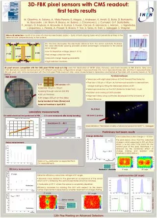
3D Sensor FBK
3D Sensor FBK. FBK / INFN Roma, November , 17 th 2009 G. Darbo - INFN / Genova. ATLAS Pixel Detector. ATLAS Pixel Detector: 3 Barrel Layers + 3 forward and backward disks. 1744 modules with 16 chips (27904 FE-I3 chips) – 1.7 m 2 of active area. Present ATLAS Pixel Detector.

3D Sensor FBK
E N D
Presentation Transcript
3D Sensor FBK FBK / INFN Roma, November , 17th 2009 G. Darbo - INFN / Genova
ATLAS Pixel Detector • ATLAS Pixel Detector: • 3 Barrel Layers + 3 forward and backward disks. • 1744 modules with 16 chips (27904 FE-I3 chips) – 1.7 m2 of active area
Present ATLAS Pixel Detector • ATLAS Pixel Module • 1744 Modules x 16 FE-I3 chips • 16.8x60.4 mm2 • Sensor • n-in-n oxygenated • 1x10¹⁵ neqcm-2 • FE-I3 • 0.13µm CMOS • 3.5 million transistors
ATLAS Pixel Pictures Bi-stave with 26 modules Layer2 half shell
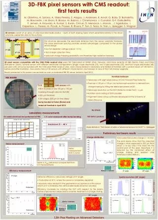
ATLAS Upgrade Plans: IBL 20.2mm 7.6mm ~200μm • Add a new layer of Pixel inside the present three layers of the detector: • 14 staves with 16 (or 32) double (single) chip modules. • Prototype 2010, production 2011÷12 • FE-I4 chip: ~2x2 cm, 250x50 µm pixel size 16.8mm ~19 mm active IBM reticule 8mm active 2.8mm ~2mm Chartered reticule (24 x 32) FE-I3 74% FE-I4 ~89% New FE-I4 Pixel size = 250 x 50 µm2 Pixels = 80 x 336 Technology = 0.13µm Power = 0.5 W/cm2 FE-I3
FE-I4 • FE-I3 not suitable for IBL • ~7% inefficiency at 3.7 cm and L = 3x1034 cm-2s-1 • FE-I3 works at 50 Mrad, but has major faults at 100 Mrad • FEI4 design collaboration formed in 2007 between: • Bonn, CPPM, Genova, LBNL, NIKHEF • FE-I4_proto chip (3/08) • Main analog blocks (3x4mm2) • Irradiated to 200 Mrad: noise increase by 20% (ENC 100120 with 400fF load and IAVDD=10µA/pixel) FE-I3 Inefficiency
IBL Requirements for Sensors/Electronics • Requirements for IBL (sensors/electronics) • IBL design Peak Luminosity = 3x1034 cm-2s-1 New FE-I4, higher hit rate • Integrated Luminosity seen by IBL = 550 fb-1 • Total NIEL dose (rmin=3.1cm): Φ1MeV = 3.1 x 10¹⁵ ± 30% (σpp) ± 50% (sensor damage factor) • Safety factor for IBL (60%) design for 5 x 10¹⁵ neq/cm2 more rad-hard sensors • Total ionization dose (TID) > 200 Mrad • ATLAS Pixel Sensor/FE-I3 designed for 1015 neq/cm2 / 50 Mrad 1MeV and TID for integrated luminosity of 1000 fb-1 Ref. Ian Dawson – ATLAS IBL General Meeting (25-26 June 09)
3D Sensors - Test Beam • Jun.09 test beam: 1 ATLAS Pixel planar, 1 3D SINTEF/Stanford (full column), 2 FBK partial double columns (FBK 3EM5 has low breakdown @ 10V) • For inclined tracks 3D sensors have similar efficiency and spatial resolution as planar – No Lorentz angle effect in 3D sensor • Active edge (STA) show efficiency up to 5÷10µm from edge • Very good collaboration between all 3D sensor producers: • Two meetings (Jun’09, Sep’09) • They look for collaboration more than competition: better chances for IBL of having compatible 3D design in time! Ref.: O. Rohne – Vertex 2009
Assemblies • Two options: module with two FE-I4 (2x4 cm2) for planar sensors or with single FE-I4 (2x2cm2) for 3D sensors • FE-I4 thickness: <350 µm (what is feasible? Prototyping with dummies) • Planar sensors thickness: 200÷300 µm • 3D sensor thickness: 230 ± 10 µm (are sensors with array of thin – 10 µm – columns, geometry similar to the FE-I3 tested assemblies) • 3D sensor could come with support wafer bonded – how can be removed after bump-deposition?
ATLAS sLHC Upgrade • For sLHC, ATLAS foresee a complete replacement of the inner detector: • Replace the Pixel with a 4 or 5 pixel layers: 2 or 3 times the surface • The two internal layers (3xIBL surface) will need material engineering (3D) or new technology (diamond) to sustain radiation fluence (2x10¹⁶ neqcm-2) • Time scale: • Prototyping: 2010÷2012 • Production: 2013÷2014 (15) • IF 3D Sensors are proven IBLtechnology, theywill find their application in ATLAS & CMSat sLHC. Two layers of “new technology” pixels Silicon Pixel Detector
Advantage of 3D vs planar • 3D sensor has several advantages over planar • More radiation hard: electrode spacing advantageous for charge collection respect to planar • More collected charge – in pixel front-end chips analog/digital crosstalk limits the lowering of threshold • Low bias voltage: 150 V vs >1000 V at high radiation dose • Low power: planar sensor need very low temperature to avoid thermal runaway • There is no Lorentz angle effect • … but the major disadvantage is a new technology • Require proof of production yield • When do we need prototypes for IBL? • FE-I4 will be submitted in March 2010 and prototype back in June • If the design is successful need sensors by mid 2010 (July) and test and irradiation in fall • Is this time schedule compatible with FBK? ….


![Industry Forecast on Global 3D Sensor Market [2014-2022]](https://cdn4.slideserve.com/7253497/slide1-dt.jpg)