Download
1 / 39
390 likes | 410 Vues
Explore the development of SiPMs by FBK-irst, highlighting key parameters, characteristics, and applications. Learn about important factors like gain, noise, and photodetection efficiency, along with detailed insights into SiPM functionalities and testing procedures. Discover the innovative FBK-irst SiPMs, their evolution, applications, and performance characteristics through collaborative efforts with research institutions. Stay informed on the latest advancements in SiPM technology and their potential applications in various fields.

E N D
Development of SiPMsa FBK-irst C.Piemonte FBK – Fondazione Bruno Kessler, Trento, Italy piemonte@fbk.eu
Outline • Important parameters of SiPM • Characteristics of FBK-irst SiPMs • Application of FBK-irst SiPM
General view of the important parameters in a SiPM • Gain • Noise • Photo-detection efficiency • Dynamic range • Time resolution
~(VBIAS-VBD)/RQ ~exp(-t/RS*CD) i exp(-t/RQ*CD) t Gain= IMAX*tQ = (VBIAS-VBD)*tQ =(VBIAS-VBD)*CD __ ________ ______________ q RQ qq Gain number of carriers produced per photon absorbed charge collected per event is the area of the exponential decay which is determined by circuital elements and bias.
NOISE 1) Primary DARK COUNT False current pulses triggered by non photogenerated carriers Main source of carriers:thermal generation in the depleted region. Critical points:quality of epi silicon; gettering techniques. 2) Afterpulsing: secondary current pulse caused by a carrier released by a trap which was filled during the primary event. 3) Optical cross-talk Excitation of neighboring cells due to the emission of photons during an avalanche discharge
micro-cell dead width Photodetection efficiency PDE= Npulses / Nphotons =QE x P01x FF 1. QEQuantum efficiency is the probability for a photon to generate a carrier that reaches the high-field region. Maximization: anti-reflective coating, drift region location 2. P01. triggering probabilityprobability for a carrier traversing the high-field to trigger the avalanche. Maximization: 1. high overvoltage 2. photo-generation in the p-side of the junction (electrons travel through the high-field region) 3. FF. Fill Factor “standard” SiPMs suffer from low FF due to the structures present around each micro-cell (guard ring, trench)
Time resolution • Statistical Fluctuations in the first stages of the current growth: • 1. Photo-conversion depth • 2. VerticalBuild-up at the very beginning of the avalanche • 3. LateralPropagation t1 t=0 pair generation 0<t<t1 drift to the high-field region t>t1 avalanche multiplication * for short wavelength light the first contribution is negligible t’1 single carrier current level the avalanche spreading is faster if generation takes place in the center
FBK-irst SiPMs • Development of SiPMs started in 2005 in • collaboration with INFN. • IRST: • development of the technology for the production of SiPMs • (large area devices/matrices) + functional characterization • INFN (Pisa, Bari, Bologna, Perugia, Trento): • development of systems, with optimized read-out electronics, • based on SiPMs for applications such as: • - tracking with scintillating fibers; • - PET; • - TOF; • - calorimetry
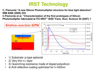
p n+ [C. Piemonte “A new Silicon Photomultiplier structure for blue light detection” NIMA 568 (2006) 224-232] IRST technology Shallow-Junction SiPM guard region n+ p p epi p+ subst. High field region Drift region 1) Substrate: p-type epitaxial 2) Very thin n+ layer 3) Polysilicon quenching resistance 4) Anti-reflective coating optimized for l~420nm
Layout: from the first design…(2005) SiPM structure: - 25x25 cells - microcell size: 40x40mm2 1mm GeometryNOT optimized for maximum PDE (max fill factor ~ 30%) 1mm
… to the new devices (i) (2007) Fill factor: 40x40mm2 => ~ 40% 50x50mm2 => ~ 50% 100x100mm2 => ~ 76% Geometries: 1x1mm2 2x2mm2 3x3mm2 (3600 cells) 4x4mm2 (6400 cells)
…to the new devices (ii) Circular: diameter 1.2mm diameter 2.8mm Matrices: 4x4 elements of 1x1mm2 SiPMs Linear arrays: 8,16,32 elements of 1x0.25mm2 SiPMs
C. Piemonte et al. “Characterization of the first prototypes of SiPM fabricated at ITC-irst” IEEE TNS, February 2007 Tests performed at FBK • IV measurement • fast test to verify functionality and uniformity of the properties. • Functional characterization in dark • for a complete characterization of the output signal and • noise properties (signal shape, gain, dark count, optical cross-talk, after-pulse) • Photo-detection efficiency
Static characteristic (IV) Reverse IV Breakdown current: determined by dark events Breakdown voltage Leakage current:mainly due to surface generation at the micro-diode periphery • Very useful fast test. Gives info about: • - Device functionality • Breakdown voltage • (Dark rate)x(Gain) uniformity • Quenching resistance(from forward IV) Performed on several thousands of devices at wafer level
Dark signals are exactly equal to photogenerated signals functional measurements in dark give a complete picture of the SiPM functioning Signal properties – NO amplifier Thanks to the large gain it is possible to connect the SiPM directly to the scope SiPM: 1x1mm2 Cell: 50x50mm2 VBIAS SiPM Digital Scope 50W
~ns Pulse gen. Laser SiPM Pulse area = charge histogram collection Signal properties – NO amplifier pedestal. 1p.e. 2 Excellent cell uniformity 3 4 Linear gain
VBIAS SiPM Digital Scope 50W Signal properties – with amplifier A voltage amplifier allows an easier characterization, but attention must be paid when determining the gain Pulses at the scope. Av 100x s = single d = double pulses a = after-pulse
Let’s look at the electro-optical characteristics of these devices: 1x1mm2 (400 cells) 4x4mm2(6400 cells) Micro-cell size: 50x50mm2
Fast transient: avalanche current through parasitic capacitance in parallel with quenching res. Slow transient: Exponential recharge of the diode capac. through the quenching resistor Signal shape 1x1mm2 SiPM - 50x50mm2 cell Set up: SiPM current signal converted into voltage on a 50W resistor and amplified with a wide-band voltage amplifier. Signal shape Important to note: The value of the quenching resistor increases with decreasing temperature and so the time constant follows the same trend
Growing threshold 1x1mm2 SiPM – 50x50mm2 cell Dark count T = -30C VBD = 27.2V From this plot we get idea of dark rate and optical cross-talk probability
2V overvoltage • 3V overvoltage • 4V overvoltage 1x1mm2 SiPM - 50x50mm2 cell Gain Dark count
Gain 16 x Dark Count of 1mm2 SiPM -15C -25C Dark count -25C -15C 4x4mm2 SiPM - 50x50mm2 cell 4x4mm2 Signal shape 1mm2 SiPM
4x4mm2 SiPM - 50x50mm2 cell T=-25C Vbd=27.6V Charge spectra when illuminating the device with short light pulses 2 3 28.6V 1 4 5 • Same conclusions as for • the previous device: • Excellent cell response uniformity • over the entire device (6400 cells) • Width of peaks dominated by • electronic noise 5 6 29.2V 4 3 2 1 6 7 5 29.6V 4 8 3 2 1
Photo-detection efficiency (2) DC curr with light DC curr. wo light dark pulses light pulses
50x50mm cell - ~50% fill factor 500nm 450nm 425nm 400nm Broad peak between 450 and 600nm …what is the PDE of these devices? Measured on 1x1mm2 SiPM using photon counting technique
Time resolution (1) • Laser:- wavelength: 400 or 800nm • - pulse width: ~60fs • - pulse period: 12.34ns withtime jitter <100fs • Filters: to have less than 1 photodetection/laser pulse • SiPMs:3 devices from 2 different batches measured G. Collazuol, NIMA, 581, 461-464, 2007.
Time resolution (2) Distribution of the time difference Timing performance (s) as a function of the over-voltage
Microcell functionality measurement (measurement at RWTH Aachen)
Microcell functionality measurement Measurement of microcell eficiency with a 5 um LED spot diameter
Some applications and projects in which we are involved
1mm SiPM matrix – for PET (1) First, small monolithic matrix of SiPM: Element 1x1mm2 Micro-cell size: 40x40mm2 IV curves of 9 matrices of one wafer 9x16 IV curves Non working SiPM • Uniform BD voltage • Uniform dark rate
SiPM matrix – for PET (2) Tests are ongoing in Pisa (DASiPM project, A. Del Guerra) on these devices coupled with pixellated and slab LSO scintillators Res = 18% Na22 spectrum with LSO on a single SiPM (1x1mm2, 40x40mm2 cell) NEXT STEP: Larger monolithic matrices
Circular SiPM - 50x50mm2 cell for CMS – Outer Hadron Calorimeter Muon response using SiPMs package designed by Kyocera 6mm2 area SiPM Muon response using HPD at 8kV module with 18 SiPMs Each SiPM reads a bundle of 5 fibers
Array of SiPM for Fiber Tracking INFN PG (R. Battiston) + Uni Aachen 32x array connected to ASIC designed for strip detectors => capacitive divider at the input to reduce signal Response uniformity under LED illumination
HYPERimage project Seventh Framework programme, FP7-HEALTH-2007-A coordinator
Development of hybrid TOF-PET/MR test systems with dramatically improved effective sensitivity First clinical whole body PET/MR investigations of breast cancer TOF-PET building blocks HYPERimage project
Conclusion • The SiPM is going to play a major role as a • detector for low intensity light, because of: • - comparable/better proprieties than PMT; • - the inherent characteristics of a solid-state det.. • IRST has been working on SiPMs (GM-APDs) for about • 3 years obtaining very good results in: • - performance; • - reproducibility; • - yield; • - understanding of the device.