Digital Design - Combinational Logic Design
Digital Design - Combinational Logic Design. Chapter 2 - Combinational Logic Design. Digital Design Combinational Logic Design.

Digital Design - Combinational Logic Design
E N D
Presentation Transcript
Digital Design - Combinational Logic Design Chapter 2 - Combinational Logic Design
Digital DesignCombinational Logic Design Figure 2.1 Motion-in-the-dark-detector system: (a) system block diagram, (b) implementation using a microprocessor, (c) implementation using a custom digital circuit.
Digital DesignCombinational Logic Design I = 9V/2 Ohms I = 4.5 A V = IR I = V/R 9V battery connected to light bulb Ohms Law
Digital DesignCombinational Logic Design • The evolution of switches: • Relays (1930s) • Vacuum tubes (1940s) • Discrete transistors (1950s) • Integrated circuit (IC) containing transistors (1960s--present). • IC’s originally held about ten transistors; now they can hold almost one billion.
Digital DesignCombinational Logic Design Figure 2.3 (b) Simple View of a Switch
Digital DesignCombinational Logic Design Figure 2.4 CMOS transistors: (left) transistor on silicon, (right top) nMOS transistor symbol with indication of conducting when gate=1, (right bottom) pMOS transistor symbol conducts when gate=0
Digital DesignCombinational Logic Design Figure 2.5 CMOS transistor operation analogy -- Crossing a river may be too difficult, until just enough stepping stones are attracted into one pathway
Digital DesignCombinational Logic Design Figure 2.6 Having the right building blocks can make all the difference when building things.
Digital DesignCombinational Logic Design Figure 2.7 Basic logic gates.
Digital DesignCombinational Logic Design 1 x 0 1 F x F 0 time NOT x F y OR x F y AND Logic Gate Behavior and Timing
Digital DesignCombinational Logic Design Figure 2.11 Timing diagram for seatbelt warning circuit Figure 2.11 Seatbelt Warning Circuit
Digital DesignCombinational Logic Design Figure 2.13 Seatbelt warning circuit with person sensor. Figure 2.14 Extended seatbelt warning circuit.
Digital DesignCombinational Logic Design • Commutative: a + b = b + a • a * b = b * a • Distributive a*(b + c) = a*b + a*c • a+(b * c) = (a+b) * (a+c) • Associative(a + b) + c = a + (b + c) • (a * b) * c = a * (b * c) • Identity 0 + a = a + 0 = a • 1 * a = a * 1 = a • Complement a + a’ = 1 • a * a’ = 0 Boolean Algebra – Basic Properties
Digital DesignCombinational Logic Design • Null elementsa + 1 = 1 • a * 0 = 0 • Idempotent Law a + a = a • a * a = a • Involution Law (a’)’ = a • DeMorgan’s Law (a + b)’ = a’b’ • (ab)’ = a’ + b’ Boolean Algebra – Additional Properties
Digital DesignCombinational Logic Design F = ab + a’ a=0 and b=0, F = 0*0 + 1 = 0 + 1 = 1 a=0 and b=1, F = 0*1 + 1 = 0 + 1 = 1 a=1 and b=0, F = 1*0 + 0 = 0 + 0 = 0 a=1 and b=1, F = 1*1 + 0 = 1 + 0 = 1 Truth Table
Digital DesignCombinational Logic Design P = a’b’c + a’bc’ + ab’c’ + abc Even Parity for Three-bit Generator
Digital DesignCombinational Logic Design Figure 2.18 Seven-segment display (left), sample numbers 0, 1 and 2 (center), and connections of inputs to segments (right)
Digital DesignCombinational Logic Design Table 2.2 4-bit binary number to seven-segment display truth table
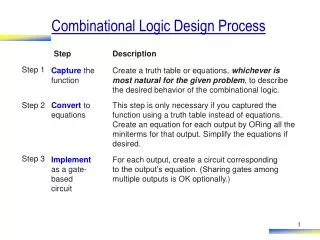
Digital DesignCombinational Logic Design Combinational Logic Design Process
Digital DesignCombinational Logic Design • Step 1: Capture the function • y = abc + bcd + cde + def + efg + fgh • Step 2: Convert to equations • Skip this as we have the equations. • Step 3: Implement as a gate-based circuit Three 1s pattern detector
Digital DesignCombinational Logic Design • Step 1: Capture the function • Step 2: Convert to equations • y = a’bc + ab’c + abc’ + abc • z = a’b’c + a’bc’ + ab’c’ + abc Number-of-1s counter gate-based circuit
Digital DesignCombinational Logic Design • Step 3: Implement as a gate-based circuit Number-of-1s counter gate-based circuit
Digital DesignCombinational Logic Design Figure 2.22 Sprinkler valve controller block diagram.
Digital DesignCombinational Logic Design • Step 1: Capture the function • d0 = a’b’c’e • d1 = a’b’ce • d2 = a’bc’e • d3 = a’bce • d4 = ab’c’e • d5 = ab’ce • d6 = abc’e • d7 = abce • Step 2: Convert to equations • Skip this as we have the equations. • Step 3: Implement as a gate-based circuit Sprinkler valve controller circuit (actually a 3x8 decoder with enable)
Digital DesignCombinational Logic Design Figure 2.24 NAND, NOR, XOR and XNOR
Digital DesignCombinational Logic Design Figure 2.25 2x4 decoder: (a) outputs for possible input combinations, (b) internal design
Digital DesignCombinational Logic Design Figure 2.26 sing a 6x64 decoder to interface a microprocessor and a column of lights for a New Year’s Eve display
Digital DesignCombinational Logic Design Figure 2.27 A multiplexer is like a railyard switch, determining which input track connects to the single output track, according to the switch’s control lever.
Digital DesignCombinational Logic Design Figure 2.28 2x1 multiplexer block symbol (left), connections for s0=0 and s0=1 (middle), and internal design (right).
Digital DesignCombinational Logic Design Figure 2.29 4x1 multiplexer block symbol (left) and internal design (right).
Digital DesignCombinational Logic Design Figure 2.30 Mayor’s vote display system implemented using a 4x1 mux.
Digital DesignCombinational Logic Design Figure 2.31 Four 2x1 muxes for selecting among 4-bit data items A or B (left), and a simpler way to represent the same component using a 4-bit 2x1 mux component (right).
Digital DesignCombinational Logic Design Figure 2.32 Above-mirror display using an 8-bit 4x1 mux.
Digital DesignCombinational Logic Design Figure 2.33 Schematic for 2x4 drawn using a popular commercial schematic capture tool.
Digital DesignCombinational Logic Design Figure 2.34 Simulation: (a) begins with us defining the inputs signal over time, (b) automatically generates the output waveforms when we ask the simulator to simulate the circuit.
Digital DesignCombinational Logic Design Figure 2.35 OR gate timing diagram: (a) without gate delay, (b) with gate delay.