Problem 4-9
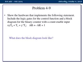
Problem 4-9. Show the hardware that implements the following statement. Include the logic gates for the control function and a block diagram for the binary counter with a count enable input xyT 0 + T 1 + y’T 2 : AR AR + 1. What does the block diagram look like?. A0. EN. A1. A2. An-1.

Problem 4-9
E N D
Presentation Transcript
Problem 4-9 • Show the hardware that implements the following statement. Include the logic gates for the control function and a block diagram for the binary counter with a count enable input xyT0 + T1 + y’T2: AR AR + 1 What does the block diagram look like?
A0 EN A1 A2 An-1 Cout Counter Block diagram
A0 EN A1 A2 An-1 Cout Control Enable, Mode, etc. xyT0 + T1 + y’T2: AR AR + 1
A0 EN A1 A2 An-1 Cout Control Enable, Mode, etc. xyT0 + T1 + y’T2: AR AR + 1
Mano 4-10 Consider the following register transfer statements for two 4-bit registers R1 and R2. xT: R1 R1 + R2 x’T: R1 R2 Draw a diagram showing the hardware implementation of the two statements. Use block diagrams for the two 4-bit registers, a 4-bit adder, and a quadruple 2-to-1-line multiplexer. In the diagram, show how the control variables x and T select the inputs of the multiplexer and the load input of register R1.
EN S A0 A1 A2 A3 B0 B1 B2 B3 Cin A0 A1 A2 A3 B0 B1 B2 B3 Y0 Y1 Y2 Y3 S0 S1 S2 S3 Cout Page 50 LD I0 I1 I2 I3 R20 R21 R22 R23 LD R2 I0 I1 I2 I3 R10 R11 R12 R13 R1 Register R1, Register R2, Quad 2x1 Mux, 4-bit adder
EN S A0 A1 A2 A3 B0 B1 B2 B3 Cin A0 A1 A2 A3 B0 B1 B2 B3 Y0 Y1 Y2 Y3 S0 S1 S2 S3 Cout LD I0 I1 I2 I3 R20 R21 R22 R23 LD R2 I0 I1 I2 I3 R10 R11 R12 R13 R10 R11 R12 R13 R1
EN S A0 A1 A2 A3 B0 B1 B2 B3 Cin A0 A1 A2 A3 B0 B1 B2 B3 T Y0 Y1 Y2 Y3 S0 S1 S2 S3 Cout xT + x’T = T LD I0 I1 I2 I3 R20 R21 R22 R23 LD R2 I0 I1 I2 I3 R10 R11 R12 R13 R10 R11 R12 R13 R1 When does R1 take on a new value?
T x 0v EN S A0 A1 A2 A3 B0 B1 B2 B3 Cin A0 A1 A2 A3 B0 B1 B2 B3 Y0 Y1 Y2 Y3 S0 S1 S2 S3 Cout Adder is connected to B-- S=1 R2 is connected to A -- S=0 LD I0 I1 I2 I3 R20 R21 R22 R23 T LD R2 I0 I1 I2 I3 R10 R11 R12 R13 R10 R11 R12 R13 R1 xT: R1 R1 + R2 x’T: R1 R2
0v T x LD EN S B0 B1 B2 B3 A0 A1 A2 A3 I0 I1 I2 I3 R20 R21 R22 R23 T Cin B0 B1 B2 B3 A0 A1 A2 A3 Y0 Y1 Y2 Y3 LD R2 I0 I1 I2 I3 R10 R11 R12 R13 S0 S1 S2 S3 Cout R10 R11 R12 R13 R1 How do the controls change if the adder is drawn differently? xT: R1 R1 + R2 x’T: R1 R2
What was left out? THE CLOCK!
0v EN S A0 A1 A2 A3 B0 B1 B2 B3 Y0 Y1 Y2 Y3 T x LD I0 I1 I2 I3 R20 R21 R22 R23 T Cin B0 B1 B2 B3 A0 A1 A2 A3 LD R2 I0 I1 I2 I3 R10 R11 R12 R13 S0 S1 S2 S3 Cout R10 R11 R12 R13 R1 xT: R1 R1 + R2 x’T: R1 R2
Guidelines: RTL hardware 1) From the register transfers, determine the values that should be connected to inputs — If a single input may be set to more than one possible value, a multiplexer must be used — The exception to the rule above occurs when all possible inputs come from three-state gates,andonly one possible input is not in the high-impedance state 2) From the condition statements, create the control signals that determine Load, Enable, Mode, etc.
Using real logic chips xyT0 + T1 + y’T2: AR AR + 1