ARM7 Architecture
ARM7 Architecture. ARM7 Core Architecture. Bus Convention. Instruction Pipelined. ARM instruction set formats. Instruction set. Instruction set. Instruction set. Addressing modes. Thumb instruction set formats. Data format. Little indian. Big indian. Operating mode.
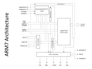

ARM7 Architecture
E N D
Presentation Transcript
Data format Little indian Big indian
Thumb registers General registers and program counter Program status registers
Program status register format Interrupt disable bits The I and F bits are the interrupt disable bits: • when the I bit is set, IRQ interrupts are disabled • when the F bit is set, FIQ interrupts are disabled
Program status register format T bit The T bit reflects the operating state: • when the T bit is set, the processor is executing in Thumb state • when the T bit is clear, the processor executing in ARM state.
Interrupt latencies The calculations for maximum and minimum latency are described in: • Maximum interrupt latencies • Minimum interrupt latencies. Maximum interrupt latencies When FIQs are enabled, the worst-case latency for FIQ comprises a combination of: Tsyncmax: The longest time the request can take to pass through the synchronizer. Tsyncmax: Is four processor cycles. Tldm: The time for the longest instruction to complete. The longest instruction is an LDM that loads all the registers including the PC. Tldm is 20 cycles in a zero wait state system. Texc: The time for the Data Abort entry. Texc is three cycles. Tfiq: The time for FIQ entry. Tfiq is two cycles.
Reset • When the nRESETsignal goes LOW a reset occurs, and the ARM7TDMI core • abandons the executing instruction and continues to increment the address bus as if still fetching word or halfword instructions. • When nRESET goes HIGH again, the ARM7TDMI processor: • 1. Overwrites R14_svc and SPSR_svc by copying the current values of the PC and CPSR into them. The values of the PC and CPSR are indeterminate. • 2. Forces M[4:0] to b10011, Supervisor mode, sets the I and F bits, and clears theT-bit in the CPSR. • 3. Forces the PC to fetch the next instruction from address 0x00. • Reverts to ARM state if necessary and resumes execution. • After reset, all register values except the PC and CPSR are indeterminate.
Bus cycles Bus cycletypes The ARM7TDMI processor bus interface is pipelined. This gives the maximum time for a memory cycle to decode the address and respond to the access request: • memory request signals are broadcast in the bus cycle ahead of the bus cycle to whichtheyrefer • address class signals are broadcast half a clock cycle ahead of the bus cycle to whichtheyrefer. Single memory cycle
Memory signals A[31:0]: is the 32-bit address bus that specifies the address for the transfer. All addresses are byte addresses, so a burst of word accesses results in the address bus incrementing by four for each cycle.The address bus provides 4GB of linear addressing space.When a word access is signaled the memory system ignores the bottom two bits, [1:0], and when a halfword access is signaled the memory system ignores the bottom bit, A[0]. All data values must be aligned on their natural boundaries. All words must be word-aligned. nRW: specifies the direction of the transfer. nRW indicates an ARM7TDMI processor write cycle when HIGH, and an ARM7TDMI processor read cycle when LOW. A burst of S-cycles is always either a read burst, or a write burst. The direction cannot be changed in the middle of a burst.
Memory signals MAS[1:0]: bus encodes the size of the transfer. The ARM7TDMI processor can transfer word, alfword, and byte quantities. All writable memory in an ARM7TDMI processor based system must support the writing of individual bytes to enable the use of the C Compiler and the ARM debug tool chain, for example Multi-ICE. The address produced by the processor is always a byte address. However, the memory system must ignore the bottom redundant bits of the address.
Memory signals nOPC: output conveys information about the transfer. An MMU can use this signal to determine whether an access is an opcode fetch or a data transfer. This signal can be used with nTRANS to implement an access permission scheme. nTRANS: output conveys information about the transfer. An MMU can use this signal to determine whether an access is from a privileged mode or User mode. This signal can be used with nOPC to implement an access permission scheme.
Memory signals LOCK: is used to indicate to an arbiter that an atomic operation is being performed on the bus. LOCK is normally LOW, but is set HIGH to indicate that a SWP or SWPB instruction is being performed. These instructions perform an atomic read/write operation, and can be used to implement semaphores. TBIT: is used to indicate the operating state of the ARM7TDMI processor. When in: • ARM state, the TBIT signal is LOW • Thumb state, the TBIT signal is HIGH.
Memory signals D[31:0], DOUT[31:0], and DIN[31:0]: The ARM7TDMI processor provides both unidirectional data buses, DIN[31:0], DOUT[31:0], and a bidirectional data bus, D[31:0]. The configuration input BUSEN is used to select which is active.