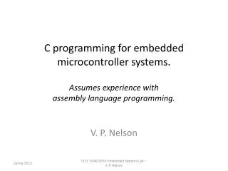
ARM7 CPU – LPC-2124 microcontroller
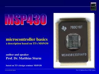
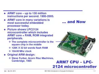
ARM7 core – up to 130 million instructions per second. 1995-2005. ARM7 core in many variations is most successful embedded processor today. Picture shows LPC2124 microcontroller which includes ARM7 core + RAM, ROM integrated peripherals.

ARM7 CPU – LPC-2124 microcontroller
E N D
Presentation Transcript
ARM7 core – up to 130 million instructions per second. 1995-2005. • ARM7 core in many variations is most successful embedded processor today. • Picture shows LPC2124 microcontroller which includes ARM7 core + RAM, ROM integrated peripherals. • The complete microcontroller is the square chip in the middle • 128K X 32 bit words flash RAM • 10mW/Mhz clock • Original ARM design: • Steve Furber, Acorn Risc Machines, Cambridge, 1985 … and Now ARM7 CPU – LPC-2124 microcontroller
I • Referencias: • “Computer Organization & Design” 2nd edition, Patterson & Hennessy 1998 (around £30 new - £15 2nd hand via Amazon) • Covers most topics on this course • V. Useful for ISE – also used in 2nd Year. • “ARM System-on-Chip Architecture”, Steve Furber, 2000 (around £25) • Best book on ARM processor
1. Levels of representation in computers temp := v[k]; v[k] := v[k+1]; v[k+1] := temp; High Level Language Program Compiler lw $15, 0($2) lw $16, 4($2) sw $16, 0($2) sw $15, 4($2) Assembly Language Program Assembler 0000 1001 1100 0110 1010 1111 0101 1000 1010 1111 0101 1000 0000 1001 1100 0110 1100 0110 1010 1111 0101 1000 0000 1001 0101 1000 0000 1001 1100 0110 1010 1111 Machine Language Program Machine Interpretation Control Signal Specification
2. What is “Computer Architecture” ? • Key: Instruction Set Architecture (ISA) • Different levels of abstraction
3. What is “Instruction Set Architecture (ISA)”? • “. ISA includes:- • Instruction (or Operation Code) Set • Data Types & Data Structures: Encodings & Representations • Instruction Formats • Organization of Programmable Storage (main memory etc) • Modes of Addressing and Accessing Data Items and Instructions • Behaviour on Exceptional Conditions (e.g. hardware divide by 0)
5. Internal Organisation Processor aka CPU (Central Processing Unit) Computer Processor Memory Devices: Control Input Datapath Output • Major components of Typical Computer System • Data is mostly stored in the computer memory separate from the Processor, however registers in the processor datapath can also store small amounts of data
CPU I/O Memory 6. Lecture 2 A Very Simple Processor The point of philosophy is to start with something so simple as not to seem worth stating, and to end with something so paradoxical that no one will believe it." Bertrand Russell • Based on von Neumann model • Stored program and data in same memory • Central Processing Unit (CPU) contains: • Arithmetic/Logic Unit (ALU) • Control Unit • Registers: fast memory, local to the CPU
MU0 - A Very Simple Processor Program Counter CPU Memory Instruction Register address data Arithmetic Logic Unit Accumulator
Logical (programmer’s) view of MU0 ADDRESS CPU Memory Memory location with address 0 is storing data 551 0 1 2 3 4 5 551 PC DATA A Registers: Each can store one number (NB IR is not visible to programmer) Memory Locations: Each can store one number
MU0 Design • Let us design a simple processor MU0 with 16-bit instruction and data bus and minimal hardware:- • Program Counter (PC) - holds address of the next instruction to execute (a register) • Accumulator (A) - holds data being processed (a register) • Instruction Register (IR) - holds current instruction code being executed • Arithmetic Logic Unit (ALU) - performs operations on data • We will only design 8 instructions, but to leave room for expansion, we will allow capacity for 16 instructions • so we need 4 bits to identify an instruction: the opcode
MU0 Design (2) • Let us further assume that the memory is word-addressible • each 16-bit word has its own location: word 0, word 1, etc. • Can’t address individual bytes! • The 16-bit instruction code (machine code) has a format: • Note top 4 bits define the operation code (opcode) and the bottom 12 bits define the memory address of the data (the operand) • This machine can address up to 212 = 4k words = 8k bytes of data
MU0 Instruction Set • mem[S] – contents of memory location with addressS • Think of memory locations as being an array – here S is the array index • A is the single 16 bit CPU register • S is a number from instruction in range 0-4095 (000(16)-FFF(16)) LoaD A Store A ADD to A SUBtract from A JuMP Jump if Gt Equal Jump if Not Equal SToP
Our First Program • The simplest use of our microprocessor: add two numbers • Let’s assume these numbers are stored at two consecutive locations in memory, with addresses 2E and 2F • Let’s assume we wish to store the result back to memory address 30 • We need to load the accumulator with one value, add the other, and then store the result back into memory 002E202F10307??? LDA 02EADD 02FSTA 030STP Note – we follow tradition and use Hex notation for addresses and data Instructions execute in sequence Human readable (mnemonic) assembly code Machine Code
MU0 addr bus PC ALU A IR data bus control Caught in the Act! Program Assembly mnemonics machine code LDA 02E 0 02E 000 2 02F ADD 02F 001 0 1 030 STA 030 002 STP 7 000 003 -- -- 004 005 -- -- -- -- 006 ... AA0 AA0 02E Data 110 110 02F -- -- 030 • Initially, we assume PC = 0, data and instructions are loaded in memory as shown, other CPU registers are undefined.
MU0 addr bus PC ALU A IR data bus control MU0 addr bus PC ALU A IR data bus control Instruction 1: LDA 02E NB – data shown is after each cycle has completed – so PC is one more than PC used to fetch instruction machine code 1 0 02E 000 2 02F 001 1 030 002 Cycle 1 (fetch instr and increment PC) 002E 7 000 003 -- 004 -- 005 -- 006 ... 1 0AA0 02E 0110 02F 0AA0 Cycle 2 (execute instruction) -- 030 002E
MU0 addr bus PC ALU A IR data bus control MU0 addr bus PC ALU A IR data bus control Instruction 2: ADD 02F machine code 2 0 02E 000 0AA0 Cycle 1 2 02F 001 1 030 002 202F 7 000 003 -- 004 -- 005 -- 006 ... 2 0AA0 02E Cycle 2 0110 02F 0BB0 -- 030 202F
MU0 addr bus PC ALU A IR data bus control MU0 addr bus PC ALU A IR data bus control Instruction 3: STA 030 machine code 3 0 02E 000 0BB0 Cycle 1 2 02F 001 1 030 002 1030 7 000 003 -- 004 -- 005 -- 006 ... 3 0AA0 02E Cycle 2 0110 02F 0BB0 0BB0 030 1030
MU0 addr bus PC ALU A IR data bus control Instruction 4: STP machine code 0 02E 000 2 02F 001 1 030 002 4 7 000 003 -- Cycle 1 004 0BB0 -- 005 -- 7000 006 ... 0AA0 02E 0110 02F 0BB0 030
Key Points: instructions • Microprocessors perform operations depending on instruction codes stored in memory • Instructions usually have two parts: • Opcode - determines what is to be done with the data • Operand - specifies where/what is the data • Program Counter (PC) - address of current instruction • PC incremented automatically each time it is used • Therefore instructions are normally executed sequentially • The number of clock cycles taken by a MU0 instruction is the same as the number of memory accesses it makes. • LDA, STA, ADD, SUB therefore take 2 clock cycles each: one to fetch (and decode) the instruction, a second to fetch (and operate on) the data • JMP, JGE, JNE, STP only need one memory read (the instruction itself) and therefore can be executed in one clock cycle.
Key Points: hardware • Memory contains both programs and data • Program area and data area in memory are usually well separated (but “self-modifying code” is possible!) • ALU is responsible for arithmetic and logic functions • There are usually one or more general purpose registers for storing results or memory addresses (MU0 only has one A – (more registers => more powerful) • Fetching data from inside the CPU is much faster than from external memory • Assume number of memory operations determines number of cycles needed to execute instruction • Assume MU0 will always reset to start execution from address 00016.
How to make CPU faster? • Make each instruction use as few clock cycles as possible • Keep as much data inside the CPU as possible (many internal registers) • Make each clock cycle as short as possible (high clock frequency) • Get each instruction to do as much as possible (?) • What do you mean by “fast”? • Different processor designs will be faster at different tasks • Use benchmarks (big standard programs) written in high level languages to compare different processors. • Processor performance is benchmark-specific
Instruction format classification • 3-operand instruction format (used by ARM processor) • dest := op1 op op2 • 2-operand instruction format (used by the Thumb instruction set of ARM, and the AVR 8 bit microcontrollers) • dest := dest op op1 • 1-operand instruction format (used in MU0 and some 8-bit microcontrollers such as MC6811) • acc := acc op op1
a := b+c REGISTORS: have e.g 8 accumulators R0-R7 a,b,c stored in memory a,b,c stored in registers LDA mem[100] ADD mem[101] STA mem[102] ADD R0,R1 MOV, R2, R0 ADD R2, R1, R0 3 operand (ARM) a: R2 b: R1 c: R0 ADD R0,R1,R2 ;R0:=R1+R2 1 operand (MU0) a: mem[102] b: mem[101] c: mem[100] 2 operand (AVR) a: R2 b: R1 c: R0 ADD R0,R1 ;R0:=R0+R1 MOV R0,R1 ;R0 := R1
RISC CISC design emphasis on compilers design emphasis on processor Design Strategies • Complex Instruction Set Computers (CISC) [e.g. VAX / ix86] • dense code, simple compiler • powerful instruction set, variable format, multi-word instructions • multi-cycle execution, low clock rate • Reduced Instruction Set Computers (RISC) [e.g. MIPS, SPARC] • high clock rate, low development cost (?) • easier to move to new technology • Simple instructions, fixed format, single-word instructions, complex optimizing compiler
Modern CPU Design • 1. Why the move from CISC to RISC? • technology factors increase expense of chip design • better compilers, better software engineers • Simple ISA better for concurrent execution • 2. Load / Store architecture • Lots of registers – only go to main memory when really necessary. • 3. Concurrent execution of instructions for greater speed • multiple function units (ALUs, etc) – superscalar or VLIW (EPIC) – examples: Pentium & Athlon • “production line” arrangement – pipeline: all modern CPU
Main memory organisation • Main memory is used to store programs, data, intermediate results • Two main organisations: Harvard & von Neumann • Harvard architecture. • In A Harvard architecture CPU programs are stored in a separate memory (possibly with a different width) from the data memory. This has the added benefit that instructions can be fetched at the same time as data, simplifying & speeding up the hardware. • In practice, the convenience of being able to read and write programs just like normal data makes this less usual • still popular for fixed program microcontrollers. CPU Instruction Memory Data Memory
Von Neumann memory architecture • Von Neumann architecture (like MU0). • Programs and data occupy a single memory. • Think of main memory as being an array of words, the array index being the memory address. Each word (array location) has data which can be separately written or read. • Usually instructions are one word in length – but can be either more or less memory bus Data & Instruction Memory Address bus CPU Control bus Data bus
Memory in detail • Memory locations store instructions data and each have unique numeric addresses • Usually addresses range from 0 up to some maximum value. • Memory space is the unique range of possible memory addresses in a computer system • We talk about “the address of a memory location”. • Each memory location stores a fixed number of bits of data, normally 8, 16, 32 or 64 • We write mem8[100], mem16[100] to indicate the value of the 8 or 16 bits with memory address 100 etc machine code 0 02E 000 2 02F 001 1 030 002 7 000 003 -- 004 -- 005 -- 006 ... 0AA0 02E 0110 02F 0BB0 030
Nibbles, Bytes, Words • Internal datapaths inside computers could be different width - for example 4-bit, 8-bit, 16-bit or 32-bit. • For example: ARM processor uses 32-bit internal datapath • WORD = 32-bit for ARM, 16-bit for MU0, 64 bit for latest x86 processors • BYTE (8 bits) and NIBBLE (4 bits) are architecture independent 31 24 23 16 15 8 7 0 MSB LSB Nibble Byte Word
Byte addresses for words • Most computer systems now use little-endian byte addressing, in which the least-significant byte has the lower address. • It is inconvenient to have completely separate byte and word addresses, so word addressing usually follows byte addressing. • The word address of a word is the byte address of its lowest numbered byte. This means that consecutive words have addresses separated by 2 (16 bit words) or 4 (32 bit words) etc. MSB LSB 4: 8: … … 16 bit memory with consecutive word addresses separated by 2 Word number Word address 3: 7 6 6: 2: 5 4 4: 3 2 1: 2: 1 0 0: 0: Not used Little-endian
Internal Registers & Memory • Internal registers (e.g. A, R0) are same length as memory word • Word READ: • A := Mem16[addr] • Word WRITE: • Mem16[addr] := A • Byte READ: • A := 00000000 Mem8[addr] • Byte WRITE: • Mem8[addr] := A(7:0) (bottom 8 bits) 16 bits bottom 8 Top 8 A 8 bits 8 bits Memory 16 bits
What are memory locations used for? LPC2138 microcontroller On-chip memory map • Read-write memory (RAM) is used for data and programs. It loses its contents on power-down. • Read-only memory (ROM) typically used to hold programs that do not change • Flash ROM allows data to be changed by programming (but not by memory write). • Memory-mapped I/O. Some locations (addresses) in memory allow communication with peripheral devices. • For example, a memory write to the data register of a serial communication controller might output a byte on a serial port of a PC. • In practice, all I/O in modern systems is memory-mapped E007 0000: I/O 28 X 16K E000 0000: 400 7FFF: RAM 32K 400 0000: 7 FFFF: ROM 512K 0:
Lecture 4 - Introduction to ARM programming “Steve is one of the brightest guys I've ever worked with – brilliant - but when we decided to do a microprocessor on our own, I made two great decisions - I gave them two things which National, Intel and Motorola had never given their design teams: the first was no money; the second was no people. The only way they could do it was to keep it really simple.” - Hermann Hauser talking about Steve Furber and the ARM design • Why learn ARM? • Currently dominant architecture for embedded systems • 32 bits => powerful & fast • Efficient: very low power/MIPS • Regular instruction set with many advanced features
Beyond MU0 - A first look at ARM • Complete instruction set. Wide variety of arithmetic, logical, shift & conditional branch instructions • Larger address space - 12-bit address gives 4k byte of memory. So use a 32-bit or address bus. • Typical physical memory size 1Mbyte (uses 20 bits) but can be anything up to 232 bytes • Subroutine call mechanism - this allows writing modular programs. • Additional internal registers - this reduces the need for accessing external memory & speeds up calculations • Interrupts, direct memory access (DMA), and cache memory. • interrupts: allow external devices (e.g. mouse, keyboard) to interrupt the current program execution • DMA: allows external high-throughput devices (e.g. display card) to access memory directly rather than through processor • Cache: a small amount of fast memory on the processor
The ARM Instruction Set • Load-Store architecture • Fixed-length (32-bit) instructions • 3-operand instruction format (2 source operand regs, 1 result operand reg): ALU operations very powerful (can include shifts) • Conditional execution of ALL instructions (v. clever idea!) • Load-Store multiple registers in one instruction • A single-cycle n-bit shift with ALU operation • “Combines the best of RISC with the best of CISC”
ARM Programmer’s Model • 16 X 32 bit registers • R15 is equal to the PC • Its value is the current PC value • Writing to it causes a branch! • R0-R14 are general purpose • R13, R14 have additional functions, described later • Current Processor Status Register (CPSR) • Holds condition codes AKA status bits r0 r1 r2 r3 r4 r5 r6 r7 r8 r9 CPSR r10 31 29 7 6 5 4 0 r11 N Z C V unused I F T mode r12 r13 (stack pointer) r14 (link register) r15 PC
ARM Programmer's Model (con't) • CPSR is a special register, it cannot be read or written like other registers • The result of any data processing instruction can modify status bits (flags) • These flags are read to determine branch conditions etc • Main status bits (AKA condition codes): • N (result was negative) • Z (result was zero) • C (result involved a carry-out) • V (result overflowed as signed number) • Other fields described later
ARM's memory organization • Byte addressed memory • Maximum 232 bytes of memory • A word = 32-bits, half-word = 16 bits • Words aligned on 4-byte boundaries NB - Lowest byte address = LSB of word “Little-endian” Word addresses follow LSB byte address 20 16 12 8 4 0
MU0 to ARM A R0 R1 R2
Introduction to ARM data processinga := b+c-d LDR R1, B LDR R2, C LDR R3, D ADD R0, R1, R2 SUB R0, R0, R3 STR R0, A ARM has 16 registers R0-R15 If a,b,c,d are in registers: LOAD data to reg from memory a: R0 b: R1 c: R2 d: R3 Machine Instructions: ADD Rx,Ry,Rz ;Rx := Ry + Rz SUB Rx,Ry,Rz ;Rx := Ry - Rz STORE result to memory from reg mem[A] mem[B] mem[C] mem[D] a b ADD R0, R1, R2 SUB R0, R0, R3 c d
An ARM assembly module module header and end symbols AREA Example, CODE ;name a code block TABSIZE EQU 10 ;defines a numeric constant X DCW 3 ; X (initialised to 3) Y DCW 11 ; Y (initialised to 11) Z % 4 ; 4 bytes (1 word) space for Z, uninitialised ENTRY ;mark start LDR r0, X ;load multiplier from mem[X] LDR r1, Y ;load number to be multiplied from mem[Y] MOV r2, #0 ;initialise sum LOOP ADD R2, R2, R1 ;add Y to sum SUB r0, r0, #1 ;decrement count CMP r0, #0 ;compare & set codes on R0 BNE LOOP ;loop back if not finished (R0 ≠ 0) STR r2, Z ;store product in mem[Z] END comments opcode operands
CMP instruction & condition codes • CMP R0, #n • computes x = R0 - n • x = 0 <=> Z = 1 • z(x) < 0 <=> N = 1 • C is carry from addition • V is two's complement overflow • BNE ;branch if Z=0 (x ≠ 0) • BEQ ;branch if Z=1 (x = 0) • BMI ;branch if N=1 (z(x) < 0) • BPL ;branch if N=0 (z(x) ≥ 0) CMP R0, #0 ; set condition codes BNE LOOP; branch if Z=0 condition codes AKA status bits N Negative Z Zero C Carry V oVerflow (signed) z(x) two complement interpretation of bits x
Two's Complement in n bit binary word unsigned binary 2n-1bn-1+ 2n-2bn-1 .... + 8b3 + 4b2 + 2b1 + b0 u(bi) 0 u 2n1 2n-1bn-1+ 2n-2bn-1 .... + 8b3 + 4b2 + 2b1 + b0 z(bi) 2n-1 s 2n-11 two's complement signed binary • Difference between z & u is not apparent in lower n bits • n bit binary addition has identical sum • carry is different • Negating two's complement is inverting bits and adding 1 • 2n does not affect lower n bits z(bi) u(bi) 2nbn-1 2n z (2n-1 z) + 1 2n-1: 11111111 z: 00000010 2n-1-z: 11111101
What is subtraction in binary? • In a microprocessor • Subtract generates correct two's complement answer for two's complement operands. • Subtract = negate followed by add: a - b = a + (-b) • Example: 4 - 1 0100 0001 - two's comp negate is invert bits & add 1: 0001 => 1110 => 1111 0100 1111 + 10011 No overflow because: cn=1 cn-1=1
Assembly module for answer AREA Example2, CODE ;name a code block S % 400 ;define 400 bytes space for table S->S+99 S1 ; S1 is label equal to S+400 ENTRY ;start instructions here MOV R0,#0 ;A := 0 ADR R2, S ;X := S ADR R9, S1 ;R9 :=S+400 for later LOOP LDR R1, [R2] ;tmp := mem[X] ADD R0, R0, R1 ;A := A + tmp ADD R2, R2, #4 ;X := X+4 CMP R2, R9 ;set condition codes on X-(S+400)? BMI LOOP ;branch back if result negative (N=1) STOP B STOP ;stop END