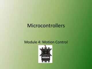
Microcontrollers ...
Microcontrollers. A microcontroller often serves as the “brain” of a system. Like a self-contained computer, it can be programmed to interact with both the hardware of the system and the user.

Microcontrollers ...
E N D
Presentation Transcript
Microcontrollers ... • A microcontroller often serves as the “brain” of a system. • Like a self-contained computer, it can be programmed to interact with both the hardware of the system and the user. • Even the most basic microcontroller can perform simple math operations, control digital outputs, and monitor digital inputs. • As the computer industry has evolved, so has the technology associated with microcontrollers.
Microcontrollers ... • Newer microcontrollers are much faster, have more memory, and have a host of input and output features that dwarf the ability of earlier models. • Most modern controllers have analog-to-digital converters, high-speed timers and counters, interrupt capabilities, outputs that can be pulse-width modulated, serial communication ports, etc.
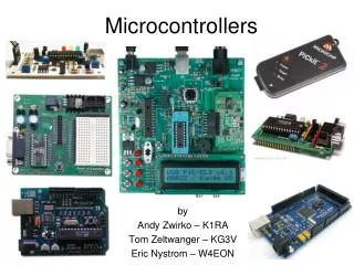
Microcontrollers ... • There are a number of popular families of microcontrollers which are used in different applications as per their capability and feasibility to perform the desired task • most common of these are • Intel’s 8051, • Atmel’s AVR and • General Instruments’ PIC microcontrollers.
Microcontrollers ... • In this class we will introduce you with AVR family of microcontrollers. • We will study one of Atmel’s AVR 8-Bit microcontrollers --- ATMega16
Resources and References • http://en.wikipedia.org/wiki/Atmel_AVR • www.atmel.com • http://www.atmel.com/Images/2466S.pdf • www.microchip.com • www.alldatasheet.com • www.avrfreaks.net
AVR microcontrollers • AVR microcontrollers are available in three categories: 1. TinyAVR – Less memory, small size, suitable only for simpler applications 2. MegaAVR – These are the most popular ones having good amount of memory (up to 256 KB), higher number of inbuilt peripherals and suitable for moderate to complex applications. 3. XmegaAVR – Used commercially for complex applications, which require large program memory and high speed.
AVR Features • The AVR --- a 8-bitRISC single chip microcontroller developed by Atmel in 1996 --- uses modified Harvard architecture . • In Harvard architecture program and data are stored in separate physical memory systems that appear in different address spaces
AVR Features ... • The AVR was one of the first microcontroller families to use on-chip flash memory for program storage, as opposed to one-time programmable ROM, EPROM, or EEPROM used by other microcontrollers at the time.
What does AVR RISC mean? • Atmel says that the name AVR is not an acronym and does not stand for anything in particular. • The creators of the AVR give no definitive answer as to what the term "AVR" stands for.
What does AVR RISC mean? .... • However, some says the acronym AVR stands for: Advanced Virtual RISC • Though, it is commonly accepted that AVR stands for Alf (Egil Bogen) and Vegard (Wollan)'s RISC processor after the names who designed the basic architecture at the Norwegian Institute of Technology when they were student.
ATMega16 Features (memory) • High Endurance Non-volatile Memory segments • 16 Kbytes of In-System Self-programmable Flash program memory • 512 Bytes EEPROM • 1 Kbyte Internal SRAM • Write/Erase Cycles: 10,000 Flash/100,000 EEPROM • Data retention: 20 years at 85°C/100 years at 25°C
ATMega16 Features ... • 32 8-bit General Purpose Working Registers • 32 Programmable I/O Lines • On-chip 2-cycle Multiplier • 8-channel, 10-bit ADC • Two 8-bit Timer/Counters with Separate Prescaler and Compare Modes • One 16-bit Timer/Counter with Separate Prescaler, Compare Mode, and Capture Mode
ATMega16 Features ... • Real Time Counter with Separate Oscillator • Four PWM Channels • Programmable Serial USART • Master/Slave SPI Serial Interface • Digital to Analog Comparator.
ATMega16 Features ... • 131 Powerful Instructions – Most Single-clock Cycle Execution • Up to 16 MIPS Throughput at 16 MHz • True Read-While-Write Operation
ATMega16 Features ... • Fully Static Operation • In-System Programming (ISP) by On-chip Boot Program • Programming Lock for Software Security • 8 Single-ended Channels • Byte-oriented Two-wire Serial Interface
ATMega16 Features ... • Special Microcontroller Features • Power-on Reset and Programmable Brown-out Detection • Internal Calibrated RC Oscillator • External and Internal Interrupt Sources • Six Sleep Modes: Idle, ADC Noise Reduction, Power-save, Power-down, Standby and Extended Standby
ATMega16 Features ... • Available in 40-Pin DIP • Operating Voltages • 4.5V - 5.5V • Speed Grades • 0 - 16 MHz
The most significant difference amongst different ATmega is the amount of “flash” storage space in the chip • which is roughly analogous to a hard drive in a PC (room for programs). • The amounts are 8kB, 16kB and 32kB. • Here’s the rub, if you don’t exceed the flash size limitation, the difference is utterly useless! • There will be no difference in execution speed, or anything else, if your code fits into a smaller size.
Pin Descriptions • Notice that most of the pins have alternate functions (shown in parentheses). • It can be found in a pdf format on Atmel’s website (www.atmel.com), AVRFreaks (http://www.avrfreaks.net/), or by searching the web.
Pin Descriptions ... • GND: Ground (0 V). Note there are 2 ground Pins. • VCC: Digital supply voltage. (+5V) • AVCC: AVCC is the supply voltage pin for Port A and the A/D Converter. • It should be externally connected to VCC, even if the ADC is not used. • If the ADC is used, it should be connected to VCC through a low-pass filter. • AREF: AREF is the analog reference pin for the A/D Converter.
Pin Descriptions ... • XTAL1 : External oscillator pin 1 • XTAL2 : External oscillator pin 2
Pin Descriptions ... Port A (PA7 -PA0) • Port A serves as the analog inputs to the A/D Converter. • Port A also serves as an 8-bit bi-directional I/O port, if the A/D Converter is not used. • When pins PA0 to PA7 are used as inputs and are externally pulled low, they will source current if the internal pull-up resistors are activated. • The Port A pins are tri-stated when a reset condition becomes active, even if the clock is not running.
Pin Descriptions ... Port B (PB7 -PB0) • Port B is an 8-bit bi-directional I/O port with internal pull-up resistors (selected for each bit). • Port B also serves the functions of various special features of the ATmega16 as listed on page 58 of datasheet.
Pin Descriptions ... Port C (PC7 -PC0) • Port C is an 8-bit bi-directional I/O port with internal pull-up resistors (selected for each bit). • Port C also serves the functions of the JTAG interface and other special features of the ATmega16 as listed on page 61 of datasheet. • If the JTAG interface is enabled, the pull-up resistors on pins PC5 (TDI), PC3 (TMS) and PC2 (TCK) will be activated even if a reset occurs.
Pin Descriptions ... Port D (PD7 -PD0) • Port D is an 8-bit bi-directional I/O port with internal pull-up resistors (selected for each bit). • Port D also serves the functions of various special features of the ATmega16 as listed on page 63 of datasheet.
Oscillator • The ATMega16 can use an internal or external clock signal • Clock signals are usually generated by an RC oscillator or a crystal • By default Atmega16 is set to operate at internal calibrated oscillator of 1 MHz. • The internal clock is an RC oscillator programmable to 1, 2, 4, or 8 MHz • The maximum frequency of internal oscillator is 8Mhz.
Oscillator • Alternatively, ATmega16 can be operated using an external crystal oscillator with a maximum frequency of 16MHz. • An external clock signal (crystal controlled) can be more precise for time critical applications • In this case you need to modify the fuse bits. (Fuse Bits will be explained later).
Architecture Diagram of Atmega16 ?
AVR CPU • PC: Program Counter • address of next instruction • IR: Instruction Register • pre-fetched instruction • ID: Instruction decoder • current instruction • GPR: R0-R31 • ALU
AVR CPU • In order to maximize performance and parallelism, the AVR uses a Harvard architecture • with separate memories and buses for program and data. • Instructions in the program memory are executed with a single level pipelining. • While one instruction is being executed, the next instruction is pre-fetched from the program memory. • This concept enables instructions to be executed in every clock cycle.
AVR CPU • The fast-access Register File contains 32 × 8-bit general purpose working registers with a single clock cycle access time. • This allows single-cycle ALU operation. • In a typical ALU operation, two operands are output from the Register File, • The operation is executed, and the result is stored back in the Register File - in one clock cycle.
AVR CPU • Six of the 32 registers can be used as three 16-bit indirect address register pointers for Data Space addressing • enabling efficient address calculations. • One of the these address pointers can also be used as an address pointer for look up tables in Flash Program memory. • These added function registers are the 16-bit X-register, Y-register, and Z-register
AVR CPU • The ALU supports arithmetic and logic operations between registers or between a constant and a register. • Single register operations can also be executed in the ALU. • After an arithmetic operation, the Status Register is updated to reflect information about the result of the operation.
AVR CPU • Program flow is provided by conditional and unconditional jump and call instructions • able to directly address the whole address space. • Most AVR instructions have a single 16-bit word format. • Every program memory address contains a 16-bit or 32-bit instruction.
AVR CPU --- ALU • The high-performance AVR ALU operates in direct connection with all the 32 general purpose working registers. • Within a single clock cycle, arithmetic operations between general purpose registers or between a register and an immediate are executed. • The ALU operations are divided into three main categories - arithmetic, logical, and bit-functions.
AVR CPU --- Status Register • The Status Register contains information about the result of the most recently executed arithmetic instruction. • This information can be used for altering program flow in order to perform conditional operations.
AVR CPU --- Status Register • Note that the Status Register is updated after all ALU operations, as specified in the Instruction Set Reference. • This will in many cases remove the need for using the dedicated compare instructions, resulting in faster and more compact code. • The Status Register is not automatically stored when entering an interrupt routine and restored when returning from an interrupt. This must be handled by software.
AVR CPU --- Status Register • • Bit 0 - C: Carry Flag • The Carry Flag C indicates a carry in an arithmetic or logic operation. • • Bit 1 - Z: Zero Flag • The Zero Flag Z indicates a zero result in an arithmetic or logic operation.
AVR CPU --- Status Register • Bit 2 - N: Negative Flag The Negative Flag N indicates a negative result in an arithmetic or logic operation. • Bit 3 - V: Two's Complement Overflow Flag The Two's Complement Overflow Flag V supports two's complement arithmetic • Bit 4 - S: Sign Bit, S = N V The S-bit is always an exclusive-OR between the Negative Flag N and the Two's Complement Overflow Flag V
AVR CPU --- Status Register • Bit 5 - H: Half Carry Flag The Half Carry Flag H indicates a Half Carry in some arithmetic operations. Half Carry is useful in BCD arithmetic • Bit 6 - T: Bit Copy Storage The Bit Copy instructions BLD (Bit LoaD) and BST (Bit STore) use the T-bit as source or destination for the operated bit. A bit from a register in the Register File can be copied into T by the BST instruction, and a bit in T can be copied into a bit in a register in the Register File by the BLD instruction
AVR CPU --- Status Register • Bit 7 - I: Global Interrupt Enable • The Global Interrupt Enable bit must be set for the interrupts to be enabled. • The individual interrupt enable control is then performed in separate control registers. • If the Global Interrupt Enable Register is cleared, none of the interrupts are enabled independent of the individual interrupt enable settings.
AVR CPU --- Status Register • The I-bit is cleared by hardware after an interrupt has occurred, and is set by the RETI instruction to enable subsequent interrupts. • The I-bit can also be set and cleared by the application with the SEI and CLI instructions • Finally, you must set the I bit in SREG enabling internal and external interrupts that have been set to operate. To stop all interrupts, just set SREG_I to 0.
Architecture Diagram of Atmega16