Microcontrollers
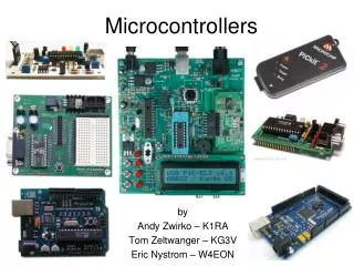
Microcontrollers. An embedded microcontroller is a chip which a computer processor with all it’s support functions (clocking and reset), memory, and i/O built into the device. Power dist. Control store. Reset control. Clock and timing. RAM. Microcontroller block diagram.

Microcontrollers
E N D
Presentation Transcript
An embedded microcontroller is a chip which a computer processor with all it’s support functions (clocking and reset), memory, and i/O built into the device. Power dist Control store Reset control Clock and timing RAM Microcontroller block diagram
types of microcontrollers • Embedded • All the hardware required to run the application is provided on the chip. typically: power, reset, clock, memory and IO. • External memory • some microcontrollers allow the connection of external memory. • Microcontroller primarily differ from a microprocessor in the areas of built-in peripheral features. These features could include memory device selection, timers, interrupt controllers, DMA, and IO devices like serial ports.
Processor Architecture • Harvard and Princeton • US govt asked for computer to be used with naval shell distance for varying elevations and environmental conditions. • Princeton provided ‘Von Neumann’ architecture where common memory space are used for storing program and data. Memory unit is responsible for arbitrary access to memory space between reading instructions and passing data back and forth with processor and its internal registers. • Advantages: simple memory interfacing and management. • Harvard proposes a design that used separate memory banks for program storage, the processor stack, and variable RAM. • Advantage: execute instruction in fewer cycles than Von Neumann.
Princeton architecture block diagram program ROM instruction decode Processor and built-in registers Data memory interface unit Variable RAM Add Ctrl Stack RAM
Harvard architecture block diagram Data program ROM instruction decode Variable RAM Add Ctrl PC Stack Processor and built-in registers Data Add Ctrl
CISC versus RISC • RISC stands for “Reduced Instruction Set Computers”. Instructions are as bare a minimum as possible to allow users to design their own operations. • CISC stands for “Complex Instruction Set Computers”. Large number of instructions, each carrying out a different permutation of the same operation.
Microcontroller memory types • control store • program memory or firmware. this memory space is the maximum size of the application that can be loaded into the microcontroller and that the application also includes all the low-level code and device interface necessary to execute an application. • nonvolatile • 8051 has 5 different types of control store : none, mask ROM, PROM, EPROM and EEPROM/Flash
variable area • 4 types variable data storage: bits, registers, variable RAM, PC stack. • in 8051 they are implemented as SRAM. • program counter stack • part of the RAM. • LIFO memory. • must be initialized by the starting address of the stack area.
Hardware interface registers (I/O space) • could be memory mapped or IO mapped. • mostly in variable memory space. memory mapped IO separate IO space program ROM program ROM IO registers IO registers IO in Princeton architecture variable RAM variable RAM Stack Counter Stack Counter
IO in Harvard architecture IO registers in program ROM IO registers in register space IO registers in separate space program ROM registers space program ROM registers space program ROM register space IO registers IO registers IO registers
Microcontroller features • clocking • IO pins • interrupts • timers • Peripherals • ADC inputs • DAC outputs • PWM outputs Basic features
interrupts Upon receipt of an interrupt: • Save the context register information • Reset the hardware requesting interrupt. • Reset the interrupt controller. • Process the interrupt. • Restore the context information. • Return to the previously executing code. Context Registers are the registers used by the interrupt during the operation of the cdoe. Exmple: addc A,@R0 during executing this code, Context registers: ACC, status register, R0 register. These are saved in Stack. Interrupt 1 8 byte data area 0000B Interrupt 0 8 byte data area 00003 8051 has two interrupts Reset vector • Priority • Nesting
Timers/counters • Event detection, timed control signal generation, counter etc. • Reads from or written to by the processor and is given by some constant frequency source. Generates an interrupt at the overflow. Run by µC clock or external clock.
8051 • several clock cycle makes an instruction cycle. 8051 instruction cycle consists of 12 clock cycles. • application should be run using slower clock speed to reduce power consumption. • Dallas version of 8051 is 87C51 has EPROM as control store and CMOS device: • 24Mhz • 12 cycle per instruction • 4Kbyte of Control stote • 128 bytes of RAM • 32 I/O lines • Two 8/16-bit times • Multiple internal and external interrupts sources • Programmable serial ports • Interface upto 128Kbytes of external memory
8051 architechture • second generation MC Basic architecture
8051 memory-register map FFFF FFFF FFFF up to 64 KB of external EPROM/ ROM up to 60 KB of external ROM/ EPROM up to 64 KB of external RAM SF = Special Function 00F8 22 SF registers 128 KB internal RAM 1000 or and 0080 007F 0FFF 4 KB of internal ROM/ EPROM 0000 0000 0000 0000 program memory data memory
About RAM • 128 bytes of internal RAM (00H to 7FH)is general R/W storage. • Part of this RAM is used as general purpose registers. • 21 Special-Function Registers (SFR) which are not part of 128 bytes of RAM at 80H to F8H locations of the RAM space. • 64 KB External RAM can be used fully in addition to 128 internal RAM. • Although 8051 normally operates with separate program and data memory space, there are applications where it can be used as one 64 KB of memory. When this is done, 8051 can input a block of data through its serial communcation port load it into memory, and then execute that data as a program.
About Program memory • if more program memory is needed, internal 4 KB memory can be expanded by an additional 60 KB, giving a full 64 KB of program memory space. • if EA (active low) is asserted, the 8051 does not use the internal 4K ROM. The external memory must start from location 0000H.
128 bytes internal RAM 7F (80) scratch pad TCON 88H 8F 88 PCON 87H F0H F7 F0 B 2F (16) bit/byte addressable DPH 83H ACC E0H E7 E0 DPL 82H PSW D0H D7 D0 IP B8H BF B8 SP 81H P3 B0H B7 B0 P0 80H 87 80 1F (8) 8-bit registers bank 3 IE A8H AF A8 A0H A7 A0 P2 SBUF PSW 99H CY AC F0 RS1 RS0 OV P 17 (8) 8-bit registers bank 2 4 register banks 98H 9F 98 SCON CY – carry flag P1 90H 97 90 AC – auxiliary carry F0 – general purpose indicator 0F (8) 8-bit registers bank 1 TH1 8DH RS1 – register bank selector bit 1 TH0 8CH RS0 – register bank selector bit 0 TL1 8BH 08 07 (8) 8-bit registers bank 0 8AH TL0 TMOD 89H
SFRs are accessed as if they were normal Internal RAM. The only difference is that Internal RAM is from address 00h through 7Fh whereas SFR registers exist in the address range of 80h through F8h. • B register is used during multiply and divide operations as to hold higher 8-bit source. Otherwise it can used as a simple scratch-pad register. • ACC and PSW are like microprocessor’s accumulator and flag. PSW does not have a zero flag. RS1 and RS0 indicates the current register bank. • DPH and DPL is used as 2-byte data pointer DTPR when addressing external memory. Can be used as 8-bit or 16 bit memory pointers. • SP incremented just before data is stored by using push or call instruction or the interrupt. 8051 SP initialized to 07H on reset. This means first data put on the stack is loaded into memory location 08H. • The 8051 has four I/O ports of 8 bits, for a total of 32 I/O lines. P0,P1,P2 and P3. • PCON is power control register. Can put mp into hibernation and conserve power.
All four 8 bit ports are bidirectional. • Port latch allows u to store data going out of the port of coming into the port. The latch can be set by data on the data bus or at the port pin. Also the latch can place data on the mc bus or send it to the port pin. • Port 0 and 2 can be used to address the external memory. Port 0 can also be used to exchange data from the external port. • Port 3 has alternative function. It’s pin 6 and 7 are used as WR/RD control for external data memory. • External program memory is read using PSEN control signal.
8051 addressing modes • 111 instructions • 49 single bytes, 45 two bytes, and 17 three-bytes. • 4 different types of instructions. • data transfer instructions. • General purpose: MOV, PUSH, POP • Accumulator specific: MOVX, MOVC, XCH • Address-object transfer: to load 16 bit address data into data pointer, e.g. MOV #data 16 • Mathematical operations. • Add, subtract, multi, divi, rotate, swap, and, or etc. • Control operations. • Call, jump, ret etc. • Bit operations. • CLR, SETB, CPL, ANL
Addressing modes • 8 addressing mode • Bank addressing, MOV A, Rn • Rn is R0 to R7 of the currently selected bank. • Direct addressing, MOV A, direct • “direct” is an internal data memory location pointed by 8 bit • Register indirect addressing, MOV A, @Ri • Ri is either R0 or R1 of the currently selected bank • Immediate addressing • 8 bit addressing, MOV A, #data • 16-bit absolute addressing, LCALL addr 16 • Addr 16 is a 16 bit absolute address in 64K locations • 11 bit relative addressing, ACALL addr 11 • Addr 11 is a 11 bit address relative to current PC value • 8 bit offset addressing, JZ rel • rel is an 8 bit offset added to current PC value. • Bit addressing, SETB bit
examples • MOV direct, direct • MOV DPTR, #data16 • MOVC A,@A+DPTR ; get content from SRAM pointed to by address A+DPTR • MOVC A, @A+PC ; get content from control store pointed to by address A+PC • MOVX A, @Ri ; get content from external RAM pointed to by Ri • MOVX A, @DPTR ; get content from external RAM pointed to by DPTR