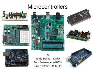
MICROCONTROLLERS
MICROCONTROLLERS. 8051. WHAT IS A MICROCONTROLLER?. All of the components needed for a controller were built right onto one chip. A microcontroller is a highly integrated chip which includes, on one chip, all or most of the parts needed for a controller.


MICROCONTROLLERS
E N D
Presentation Transcript
MICROCONTROLLERS 8051
WHAT IS A MICROCONTROLLER? • All of the components needed for a controller were built right onto one chip. • A microcontroller is a highly integrated chip which includes, on one chip, all or most of the parts needed for a controller. • The microcontroller could be called a "one-chip solution".
Features : • The Intel 8051 is used in embedded systems • 8-bit CPU • 4k bytes ROM for the program • 128 BYTES of RAM • 32 I/O lines ( 4 PORTS WITH 8 EACH ) • 2 timers • 1 Serial port • 6 interrupt sources • Low cost (10-15 cents per chip)
Block Diagram External Interrupts Interrupt Control 4k ROM 128 bytes RAM Timer 1 Timer 2 CPU OSC Bus Control 4 I/O Ports Serial RXD P0 P2 P1 P3 TXD Addr/Data
8051 contains four I/O ports (P0 - P3) • Each port can be used as input or output (bi-direction)
IMPORTANT PINS • PSEN (out): Program Store Enable, the read signal for external program memory (active low). • ALE (out): Address Latch Enable, to latch address outputs at Port0 and Port2 • EA (in): External Access Enable, active low to access external program memory locations 0 to 4K • RXD,TXD: UART pins for serial I/O on Port 3 • XTAL1 & XTAL2: Crystal inputs for internal oscillator.
SIGNALS - OPERATION • Vcc(pin 40): • Vcc provides supply voltage to the chip. • The voltage source is +5V. • GND(pin 20):ground • XTAL1 and XTAL2(pins 19,18): • These 2 pins provide external clock. using a quartz crystal oscillator
C2 XTAL2 30pF C1 XTAL1 30pF GND QUARTZ CRYSTAL OSCILLATOR • Using a quartz crystal oscillator • We can observe the frequency on the XTAL2 pin.
RST - RESET • RST(pin 9):reset • input pin and active high • The high pulse must be high at least 2 machine cycles. • power-on reset. • Upon applying a high pulse to RST, the microcontroller will reset and all values in registers will be lost. • Reset values of some 8051 registers
RESET Value of Some 8051 Registers: Register Reset Value PC 0000 ACC 0000 B 0000 PSW 0000 SP 0007 DPTR 0000 RAM are all zero
Vcc 31 EA/VPP X1 10 uF 30 pF X2 RST 9 8.2 K RESET CIRCUITARY
BLOCK DESCRIPTION • ACCUMULATOR ( ACC ) • Operand register • Implicit or specified in the instruction • Has an address in on chip SFR bank • B REGISTER • to store one of the operands for multiplication and division • otherwise, scratch pad • considered as a SFR
PROGRAM STATUS WORD ( PSW ) • Set of flags contain status information • One of the SFR • STACK POINTER ( SP ) • 8 bit wide register • Incremented before data is stored on to the stack using PUSH or CALL instructions • Stack defined anywhere on the 128 byte RAM • RESET initiated to 0007H • Not a top to down structure • Allotted an address in SFR
DATA POINTER ( DPTR ) • 16 bit register • contains DPH and DPL • Pointer to external RAM address • DPH and DPL allotted separate addresses in SFR bank • PORT 0 TO 3 LATCHES & DRIVERS • Each i/o port allotted a latch and a driver • Latches allotted address in SFR • User can communicate via these ports • P0, P1, P2,P3
SERIAL DATA BUFFER • internally had TWO independent registers • TRANSMIT buffer parallel in serial out ( PISO ) • RECEIVE buffer serial in parallel out (SIPO) • identified by SBUF and allotted an address in SFR • byte written to SBUF initiates serial TX • byte read from SBUF reads serially received data • TIMER REGISTERS • for Timer0 ( 16 bit register – TL0 & TH0 ) • for Timer1 ( 16 bit register – TL1 & TH1 ) • four addresses allotted in SFR
OSCILLATOR • generates basic timing clock signal using crystal oscillator • INSTRUCTION REGISTER • decodes the opcode and gives information to timing and control unit • EPROM & PROGRAM ADDRESS REGISTER • provide on chip EPROM and mechanism to address it • All versions don’t have EPROM • RAM & RAM ADDRESS REGISTER • provide internal 128 bytes RAM and a mechanism to address internally
ALU • Performs 8 bit arithmetic and logical operations over the operands held by TEMP1 and TEMP 2 • User cannot access temporary registers • SFR REGISTER BANK • set of special function registers • address range : 80 H to FF H
INSTRUCTIONS SET • ARITHMETIC INSTRUCTIONS • LOGIC INSTRUCTIONS • BOOLEN INSTRUCTIONS • DATA TRANSFER INSTRUCTIONS • SINGLE BIT INSTRUCTIONS • JUMP,LOOP AND CALL INSTRUCTIONS
Arithmetic instructions ADD,SUB,DIV,MUL,INC,DEC
ADD & SUB add a, byte ; a a + byte addc a, byte ; a a + byte + C These instructions affect 3 bits in PSW: C = 1 if result of add is greater than FF AC = 1 if there is a carry out of bit 3 OV = 1 if there is a carry out of bit 7, but not from bit 6, or visa versa.
ADD Example • What is the value of the C, AC, OV flags after the second instruction is executed? mov a, #3Fh add a, #D3h 0011 1111 1101 0011 0001 0010 C = 1 AC = 1 OV = 0
Subtract Example: SUBB A, #0x4F ;A A – 4F – C Notice that There is no subtraction WITHOUT borrow. Therefore, if a subtraction without borrow is desired, it is necessary to clear the C flag. Example: Clr c SUBB A, #0x4F ;A A – 4F
Increment & Decrement • The increment and decrement instructions do NOT affect the C flag. • Notice we can only INCREMENT the data pointer, not decrement.
SIGNIFICANCE OF carry flag • Assume 16-bit word in R3:R2mov a, r2 add a, #1 ; use add rather than increment to affect C mov r2, a mov a, r3 addc a, #0 ; add C to most significant byte mov r3, a
Multiply When multiplying two 8-bit numbers, the size of the maximum product is 16-bits FF x FF = FE01 (255 x 255 = 65025) MUL AB;BA A * B Note : B gets the High byte A gets the Low byte
Division • Integer Division DIV AB ; divide A by B A Quotient(A/B) B Remainder(A/B) OV - used to indicate a divide by zero condition. C – set to zero
Decimal Adjust DA a; decimal adjust a Used to facilitate BCD addition. Adds “6” to either high or low nibble after an addition to create a valid BCD number. Example: mov a, #23h mov b, #29h add a, b; a 23h + 29h = 4Ch(wanted 52) DA a ; a a + 6 = 52
BOOLEAN INSTRUCTIONS CLR,CPL,SETB,AND,OR
BOOLEAN INSTRUCTIONS • This group of instructions is associated with the single-bit operations of the 8051. • This group allows manipulating the individual bits of bit addressable registers and memory locations as well as the CY flag. • The P, OV, and AC flags cannot be directly altered. • This group includes: • Set, clear, and, or complement, move. • Conditional jumps.
CLR <bit> CLR C CLR bit CLR instruction can operate on any directly addressable bit CLR P2.7 If Port 2 has been previously written with DCH (11011100), then the operation leaves the port set to 5CH (01011100) • CLR instruction can operate on the carry flag • CLR C • The CARRY flag is set to 0
SETB <bit> SETB C SETB bit SETB instruction operates on any directly-addressable bit and sets the specified bit to 1 SETB P2.0 Port 2 has the value of 24H (00100100), the Port 2 value changes to 25H (00100101) • SETB instruction operates on the carry flag and sets the specified bit to 1 • SETB C • sets the carry flag to 1
CPL <bit> CPL C CPL bit CPL instruction complements any directly addressable Bit CPL P2.2 If Port 2 has the value of 53H (01010011) then after the execution the port set to 55H (01010101) • This operation complements the carry flag • CPL C
ANL ANL C, <source-bit> ANL C, /<source-bit> If a slash (/) is used in the source operand bit, the logical complement of the source bit is used, but the source bit itself is not affected ANL C,/OV ;AND with inverse of OV flag • This instruction ANDs the bit addressed with the carry bit and stores the result in the carry bit itself • ANL C,P2.7 ;AND carry flag with bit 7 of P2
ORL ORL C, <source-bit> ORL C, /<source-bit> If a slash (/) is used in the source operand bit, the logical complement of the source bit is used, but the source bit itself is not affected ORL C,/OV ;OR with inverse of OV flag • This instruction ORs the bit addressed with the carry bit and stores the result in the carry bit itself • ORL C,P2.5 ;OR carry flag with bit 5 of P2
MOV <dest-bit>,<source-bit> • One of the operands must be the carry flag; the other may be any directly-addressable bit MOV C,P3.3 MOV P2.0,C • If P2=C5H (11000101), P3.3=0 and CY=1 initially, after instructions, P2=C4H (11000100) and CY=0
JC / JNC addr • Jump to a relative address if CY is set / cleared.
JB / JNB <bit>,addr • Jump to a relative address if a bit is set / cleared.
JBC <bit>,addr • Jump to a relative address if a bit is set and clear the bit. JBC P1.3,ARRAY1 • If P1=56H (01010110), the above instruction sequence will cause the program to branch to the instruction at ARRAY1, modifying P1 to 52H (01010010)
BRANCH INSTRUCTIONS CALL, JMP, RET
Branching instructions • Program branching instructions are used to control the flow of actions in a program • Some instructions provide decision making capabilities and transfer control to other parts of the program. • e.g. conditional and unconditional branches
CALL ACALL & LCALL • The 8051 provides 2 forms for the CALL instruction: • Absolute Call – ACALL • Uses an 11-bit address • The subroutine must be within the same 2K page. • Long Call – LCALL • Uses a 16-bit address • The subroutine can be anywhere. • Both forms push the 16-bit address of PC on the stack and update the stack pointer.
Absolute Call – ACALL addr11 • This instruction unconditionally calls a subroutine indicated by the address • 2 byte instruction: The upper 3-bits of the address combine with the 5-bit opcode to form the 1st byte and the lower 8-bits of the address form the 2nd byte Eg. ACALL LOC_SUB • If SP=07H initially • label “LOC_SUB” is at memory 0567H, • then executing instruction at 0230H (PC), • SP=09H, internal RAM locations 08H and 09H will contain 32Hand 02H respectively and PC=0567H
LONG CALL - LCALL addr16 • It is a Long call, the subroutine may therefore begin anywhere in the full 64 kB program memory address space • 3 byte instruction LCALL LOC_SUB • Initially, SP=07H • label “LOC_SUB” is at memory 4100H • Executing the instruction at 0230H ( PC), • SP=09H, internal RAM locations 08H and 09H contain 33H and 02H respectively and PC=4100H
RETURN RET & RETI • The 8051 provides 2 forms for the return instruction: • Return from subroutine – RET • Pop the return address from the stack and continue execution there. • Return from ISR – RETI • Pop the return address from the stack. • Restore the interrupt logic to accept additional interrupts at the same priority level as the one just processed. • Continue execution at the address retrieved from the stack. • The PSW is not automatically restored.
JUMP SJMP • The 8051 provides four different types of unconditional jump instructions: • Short Jump – SJMP addr • Uses an 8-bit signed offset relative to the 1st byte of the next instruction. • the range of destination allowed is from -128 to+127 bytes from the instruction SJMP RELSRT • If the label RELSRT is at program memory location 0120H and the SJMP instruction is located at address 0100H ( PC) ,after executing the instruction, PC=0120H