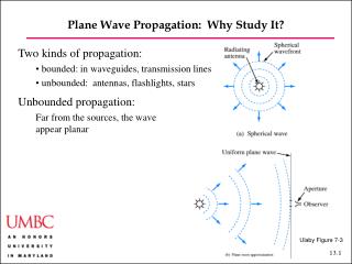
Plane wave scattering on a stratified layer
200 likes | 330 Vues
This guide details the computation of plane wave scattering on a 100nm thick gold layer illuminated by a p-polarized plane wave at 1070nm. Utilized within Lumerical GIST, it describes the steps to set up the simulation, including creating regions, defining boundary conditions, and configuring the material properties. It also addresses a common error related to processor layout and provides solutions for adjusting mesh resolution. Finally, it guides the visualization of the electric field distribution and comparison with analytic solutions.

Plane wave scattering on a stratified layer
E N D
Presentation Transcript
Plane wave scattering on a stratified layer Computation using Lumerical GIST, Prof. Yong-Gu Lee 20141009
Objective • 100nm thick gold layer is illuminated with a plane wave @1070nm p-polarized in the orthogonal direction. Compute the total electric field distribution.
LauchLumerical FDTD and start from an empty object layout, create a region Toolbar: Simulation->Region Object tree: FDTD->Right mouse 2D simulation Medium is water with index of refraction 1.33 X span 100nm, Y span 200 nm
Create a mesh of particular width and depth Toolbar: Simulation->Mesh Object tree: mesh->Right mouse X span 100nm, Y span 200 nm
Create a gold substrate Double click Quadrilateral X span 150nm, Y span 100 nm
Set boundary conditions Bloch boundary condition in the x-axis
Set the material for the substrate Au (Gold) – Johnson and Christy
Second oops Drexler(process 0): The program terminated due to an error:There is no possible parallel processor layout that can be used because the simulation volume is too small. Please reduce the number of processors or contact Lumerical Technical Support for more information.
Mesh resolution problem Change x mesh from 15 nm to 1 nm