Stacking Process
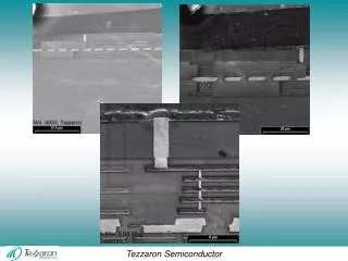
Stacking Process. < Optical Micrograph >. < Scanning Electron Micrograph >. 3 rd Si thinned to 5.5um. 2 nd Si thinned to 5.5um. SiO 2. 1 st Si bottom supporting wafer. “Super Via” 4um in diameter and 12um in height. Three wafers successfully aligned and stacked. 3 rd Si

Stacking Process
E N D
Presentation Transcript
Stacking Process < Optical Micrograph > < Scanning Electron Micrograph > 3rd Si thinned to 5.5um 2nd Sithinned to 5.5um SiO2 1st Si bottom supporting wafer “Super Via” 4um in diameter and 12um in height Three wafers successfully aligned and stacked
3rd Si 2nd Si 1st Si
1.2 um Si 2nd wafer 4.8 um 2 um 2 um SiO2 Cu Si 1st wafer Exposed Bottoms of Super Vias Microscope View Profiler View Wet Etch: 1.2 µm Copper Via protruding
3rd Wafer Blanket Cu Super Via Top Metal Pad 2nd Wafer pattern Cu 1st Wafer Blanket Cu Three Cu Wafer Stacking FIB micrograph showing 3 stacked wafer using newly designed process flow Three wafers stacking using an alternative stacking architecture “stacking process without backside process” invented during this project time, has been successfully demonstrated.
Reg. File / Mixed Signal ASIC • Byte per layer dual port memory • Bandgap on each layer • Heater Resistor to induce stress • 133MHz DLL (DDRI/II) • 4 Stage charge pump (cross layer) • POR
CPU/Memory Stack • R8051 CPU • 80MHz operation; 140MHz Lab test (VDD High) • 220MHz Memory interface • IEEE 754 Floating point coprocessor • 32 bit Integer coprocessor • 2 UARTs, Int. Cont., 3 Timers, … • Crypto functions • 128KBytes/layer main memory • Completely synthesized, placed and routed in 3D with standard Cadence tools. Runs slightly better than predicted by models and tools.