Silicon strip detectors and their readout electronics
510 likes | 771 Vues
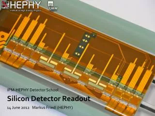
Silicon strip detectors and their readout electronics. Francis Anghinolfi CERN. OUTLINE. Silicon strips detectors for tracking (Micro)Electronics for silicon strips Strips readout examples. NB : I will not talk about silicon pixel detectors nor silicon drift detectors ….

Silicon strip detectors and their readout electronics
E N D
Presentation Transcript
Silicon strip detectors and their readout electronics Francis Anghinolfi CERN F. Anghinolfi CERN/PH/ESE Seminar
OUTLINE • Silicon strips detectors for tracking • (Micro)Electronics for silicon strips • Strips readout examples NB : I will not talk about silicon pixel detectors nor silicon drift detectors ….. F. Anghinolfi CERN/PH/ESE Seminar
Silicon Strips Detectors PROS • Solid State • ~100% efficient for particle detection • Small (best when ….) CONS • No multiplication Small signals, then need smart electronics to detect the signal (large amplification and noise reduction) • Leakage (DC) current F. Anghinolfi CERN/PH/ESE Seminar
Silicon Strips Detectors Solid state • No gas, no liquid stable material • But as a consequence, subject to radiation degradation • Benefits from silicon wafer industry environment (access to very pure silicon material, precise alignment machines, clean room technologies etc …) F. Anghinolfi CERN/PH/ESE Seminar
Silicon Strips Detectors Efficiency SIGNAL if there is PARTICLE Detection Efficiency close to 100% Charge is always generated by a MIP crossing particle F. Anghinolfi CERN/PH/ESE Seminar
Silicon Strips Detectors Efficiency SIGNAL if there is PARTICLE Detection Efficiency close to 100% • Inefficiency may result from : • Insensitive areas (edges) • Charge sharing • Traps or defect F. Anghinolfi CERN/PH/ESE Seminar
Silicon Strips Detectors Signal formation in Silicium - - - - - c ++++ • High Energy Particle deliver signal in the depletion region, by electron hole pair creation. • Positive and negative charges drift in presence of the applied electric field F. Anghinolfi CERN/PH/ESE Seminar
Silicon Strips Detectors Signal formation in Silicium • The depletion region is obtained by applying a voltage between top and bottom of the detector • For large voltage and small doping concentration it is possible to obtain the depletion of the full volume F. Anghinolfi CERN/PH/ESE Seminar
Silicon Strips Detectors Signal formation in Silicium The diode (p-type over n-type bulk in this figure) is needed to block direct current path. Direct current path could be as high as mA per strips ( a killer for signal detection) The diode is reverse biased. The dynamic signal from particle track is sensed through the capacitance of the blocking diode F. Anghinolfi CERN/PH/ESE Seminar
Silicon Strips Detectors Signal formation in Silicium • The signal is formed by electron-hole pair creation along the track path • for a fully depleted silicon volume 300 um thick the average signal is around 22000 electrons (3.5 fC) The energy loss for a Minimum Ionizing Particle (MIP) is around 260eV/um for 300um thick silicon. One e-h pair creation energy in silicon is 3.62 eV F. Anghinolfi CERN/PH/ESE Seminar
Silicon Strips Detectors Charge sharing e- e- e- e- e- e- Strip pitch Collected Charge quantity depends on the depleted silicon thickness In case of track angle the charge distributes on adjacent strips Strip length The charges are drifting along the electrical field toward the strips. The electronics channels are connected to the strips (directly or through decoupling capacitors) Particle track through Si material F. Anghinolfi CERN/PH/ESE Seminar
Silicon Strips Detectors Signal formation in Silicium • The collection time is usually below 10ns for electrons (drifting to one side) and below 25ns for holes (drifting the other side) • Good time resolution is also possible • (~ few ns range, OK for LHC with 25ns bunch interval) F. Anghinolfi CERN/PH/ESE Seminar
Silicon Strips Detectors The Signal is small For example read the signal on 50 ohms resistor : Typical 3.5fC delivered on 50 ohms in ~10ns results in peak voltage of 17uV The voltage noise of the 50 ohms resistor in the bandwidth required for signal is ~ 3.5uV rms The ratio (5), is not enough to provide safe signal detection (additional noise sources, charge sharing etc …) F. Anghinolfi CERN/PH/ESE Seminar
Silicon Strips Detectors The sensing geometry (strip size) can be small • Small is good for tracking detectors : 10-20um position resolution attainable (less for pixels) • Small geometry is beneficial for the signal detection electronics …. F. Anghinolfi CERN/PH/ESE Seminar
Silicon Strips Detectors Small is good for the detection • Small areas are obtained by the detector segmentation • There is no signal loss (dead areas) even with segmented detectors • Small areas have less leakage current and less capacitance, 2 key items which improve the signal detection (signal over noise ratio SNR) F. Anghinolfi CERN/PH/ESE Seminar
Silicon Strips Detectors Example : Segmented detector This detector is made of 4 rows of 1280 strips of length 2,5cm. The strip pitch (horizontal axis) is 80um. The expected resolution is 23 um in X. (Development for ATLAS upgrade, KEK, Japan) 4 rows of 2.5cm long strips 2,5cm 1280 strips on ~ 10 cm F. Anghinolfi CERN/PH/ESE Seminar
Silicon Strips Detectors What we know about electronics for Silicon Strips • Has to deal with small signal and leakage current • Small detector segments have less leakage current and less capacitance, 2 key items which improve the signal detection (signal over noise ratio SNR) • But more channels to cover a fixed detecting area : • It creates a trade-off between power (nbe of channels) versus SNR F. Anghinolfi CERN/PH/ESE Seminar
+ Rp Z - Electronic Circuit Particle Detector Readout Electronics Typical “front-end” elements The electronics circuit is necessary for : signal amplification (signal multiplication factor) noise rejection signal “shaping” Impedance adaptation Final objective : Signal detection Amplitude measurement Time measurement F. Anghinolfi CERN/PH/ESE Seminar
Readout Electronics Circuit • Impedance adaptation • Amplitude resolution • Time resolution • Noise cut High Z Low Z Voltage source + Zo Z Rp - Low Z T Low Z output voltage source circuit can drive any load Output signal shape adapted to subsequent stage (T/H, ADC, Discriminator) Signal shaping is used to reduce noise vs. signal F. Anghinolfi CERN/PH/ESE Seminar
Readout Electronics x(f) y(f) h(f) x(f) y(f) f f f0 Noise floor (white) f0 Improved Signal/Noise Ratio f f0 Example of signal filtering : the above figure shows a « standard » filter case, where only noise is filtered out. F. Anghinolfi CERN/PH/ESE Seminar
Readout Electronics x(f) y(f) h(f) x(f) y(f) f f Noise floor f0 Improved Signal/Noise Ratio f f0 In particle physics, the input signal, from detector, is often a very fast pulse, similar to a “Dirac” pulse. Therefore, its frequency representation is over a large frequency range. The filter (shaper) provides a limitation in the signal bandwidth and therefore signal shape at the filter output is different from the input signal shape. • The output signal shape, different from the input detector signal shape, is chosen to optimize the Signal-to-Noise Ratio • Doing this there is a trade-off btw. SNR, power and pile-up F. Anghinolfi CERN/PH/ESE Seminar
Readout Electronics Filter cuts noise. Signal BW is preserved f f0 Filter cuts inside signal BW : modified shape f f0 F. Anghinolfi CERN/PH/ESE Seminar
Readout Electronics Preamplifier Shaper I O d(t) Q/C.n(t) • What are the functions of preamplifier and shaper (in ideal world) : • Preamplifier : is an ideal integrator : it detects an input charge burst Q d(t).The output is a voltage step Q/C.n(t). Has large signal gain such that noise of subsequent stage (shaper) is negligeable. • Shaper : a filter with : characteristics fixed to give a predefined output signal shape, and rejection of noise frequency components which are outside of the signal frequency range. F. Anghinolfi CERN/PH/ESE Seminar
f f Readout Electronics Preamplifier Shaper I O t t Q/C.n(t) d(t) CR_RC4 shaper Ideal Integrator T.F. from I to O 1/s RCs /(1+RCs)5 = RC/(1+RCs)5 = x Output signal of preamplifier + shaper with “ideal” charge at the input t F. Anghinolfi CERN/PH/ESE Seminar
Readout Electronics Shaper Preamplifier I O Non-Ideal Integrator CR_RC shaper d(t) Integrator baselinerestoration x 1/(1+T1s) RCs /(1+RCs)2 Non ideal shape, long tail F. Anghinolfi CERN/PH/ESE Seminar
Readout Electronics Preamplifier Shaper I O Non-Ideal Integrator CR_RC shaper d(t) Integrator baselinerestoration T.F. from I to O 1/(1+T1s) x (1+T1s) /(1+RCs)2 Pole-Zero Cancellation Ideal shape, no tail F. Anghinolfi CERN/PH/ESE Seminar
Readout Electronics • Pile-up • The detector pulse is transformed by the front-end circuit to obtain a signal with a finite return to zero time CR-RC : Return to baseline > 7*Tp 1 2 3 4 5 8 7 CR-RC4 : Return to baseline < 3*Tp 2 3 1 F. Anghinolfi CERN/PH/ESE Seminar
Readout Electronics For the requirement of strips readout for the LHC experiments, the shaping (peaking) time should be in the order of 25 ns It allows discrimination of events as close as 75ns With the CR-RCn circuits as described above, it is difficult to trade 25ns peaking time with low power circuit F. Anghinolfi CERN/PH/ESE Seminar
Readout Electronics • Different solutions have been implemented to realize low power and fast (25ns) shaping time for the LHC experiments: • transimpedance amplifiers • analog signal processing F. Anghinolfi CERN/PH/ESE Seminar
Readout Electronics For ideal Amplifier A Transimpedance Amplifier Resistive feedback element The main pole is function of the detector input capacitance Other poles are coming from the amplifier open-loop transfer function. The preamplifier does a fraction of the shaping function But this circuit is critically stable and needs careful design The feedback element Rf contributes to the noise Rf iin(t) A Vout Cd Amplifier Detector model F. Anghinolfi CERN/PH/ESE Seminar
1 of the 128 channels programmable gain differential current output stage unity gain inverter 128:1 MUX analogue pipeline S/H APSP SF SF charge preamplifier shaper Readout Electronics Analogue Signal Processing Analogue sampling and storage Analog Processor, 25ns shaping time Charge preamp 50ns shaper The fastshapingisappliedonly to selectedsamples of the signal, thereforethereis a gain in power F. Anghinolfi CERN/PH/ESE Seminar
4kTRs Rs G(f) 2qIshot Rp Cd 4kTRp Readout Electronics The Signal-to-Noise Ratio Whatever is the solution choosen to realize the shaping function, the overall Signal-to-Noise depends on the overall electronics circuit transfer function up to the measurement output The signal is from the detector, the noises are from the active (transistor, diode) and passive (resistors) elements Resistance in serie Input transistor (under assumption that load does not contribute, and that the input gain stage is high enough to neglect 2nd stages contribution…) Resistance in parallel Diode (for strips : reverse bias diode) F. Anghinolfi CERN/PH/ESE Seminar
4kTRs Rs G(f) 2qIshot Rp Cd 4kTRp Readout Electronics The Signal-to-Noise Ratio In case of strips : Input device “channel” noise Not present Strip capacitance Front-end circuit with shaping time constant t Bias resistors Reverse bias diode leakage F. Anghinolfi CERN/PH/ESE Seminar
Readout Electronics The Signal-to-Noise Ratio • All noise contributions are calculated in terms of noise voltage appearing at the input of the amplifier • Noise sources are from detector element and from amplifier. 4 noise sources are considered here : • Ishot current in diode (leakage current in Si Detector element ) • Rp noise, (any) resistance in parallel to the input • Rs noise, (any) resistance in serie with the input • V2na equivalent input noise of the input device of the amplifier F. Anghinolfi CERN/PH/ESE Seminar
4kTRs Rs G(f) 2qIshot Rp Cd 4kTRp Readout Electronics The Signal-to-Noise Ratio t is the shaping time (0 to peak) of the CR_RC2 shaping function V2nais the equivalent voltage noise source of the amplifier input device A formulation of the noise in “electrons” is given here for the CR-RC2 transfer function G(f) The signal-to noise ratio is computed by division of the signal expressed in electrons by the ENC calculated with the formula gmis proportional to the square root of the current in the input device F. Anghinolfi CERN/PH/ESE Seminar
n n 1 1 2 2 3 3 4 4 5 5 6 6 7 7 Fs Fp 0.92 0.92 0.84 0.63 0.95 0.51 0.45 0.99 1.11 0.40 1.16 0.36 1.27 0.34 Readout Electronics To reduce ENC The Signal-to-Noise Ratio Increase transistor current (power !) Formulation without diode current, without Rs Small detector segment Shaping time trade-off CR-RCn “n” factor dependance F. Anghinolfi CERN/PH/ESE Seminar
Readout Electronics The Signal-to-Noise Ratio ENC (el.) ENC (el.) C=15pF optimum C=10pF C=5pF Shaping time (ns) Shaping time (ns) ENC dependence to the shaping time (C=10pF, gm=10mS, R=100Kohms) F. Anghinolfi CERN/PH/ESE Seminar
Readout Electronics The Power vs. other parameters trade-off This (approximate, don’t use it in real life !) equation shows the relationship btw. the front-end power (input branch only !), detector capacitance and noise performance Numerical example : Target 10pF detector, ENC as 500el. t=25ns, V= 2.5V P = 0.32mW (strips typical) Target 0.2pF detector, ENC as 120el. t=25ns, V= 2.5V P = 3 mW (pixel case) F. Anghinolfi CERN/PH/ESE Seminar
pipeline 128x192 APSP + 128:1 MUX 128 x preamp/shaper 7.1mm control logic bias gen. FIFO pipe logic CAL 8.1 mm Readout System for highly segmented Si Strips detectors APV25 description • The CMS silicon tracker analogue architecture; • 128 channels of preamplifier/shaper followed by one analogue memory (pipeline) bank. • The APSP is the final “fast” shaping circuit, acting on selected signal samples • The readout is analogue : reading amplitude allows to measure charge sharing across adjacent strips F. Anghinolfi CERN/PH/ESE Seminar
Readout System for highly segmented Si Strips detectors ABCD/N description • The ATLAS silicon tracker binary architecture; • 128 channels of preamplifier/shaper/comparator with two memory banks, one for trigger latency and one readout buffer • The readout is binary (either above or below a programmable threshold). Low threshold setting is required to not loose signal in case of charge sharing F. Anghinolfi CERN/PH/ESE Seminar
Readout System for highly segmented Si Strips detectors Beetle FE chip • The LHCb VELO frontend chip tracker has • 128 channels of preamplifier/shaper/discriminator followed by one analogue memory (pipeline) bank. Either analogue or binary data is stored into the pipeline. • The readout is analogue but both amplitude or binary information can be readout. F. Anghinolfi CERN/PH/ESE Seminar
Readout System for highly segmented Si Strips detectors Performance and system aspects for the LHC experiments F. Anghinolfi CERN/PH/ESE Seminar
Readout System for highly segmented Si Strips detectors PHOTOS • The VELO tracker detector of LHCb: • The electronics (Beetle) are on the PCB circling around the radial strips F. Anghinolfi CERN/PH/ESE Seminar
Readout System for highly segmented Si Strips detectors PHOTOS • The CMS tracker module : • Two large planes detectors are connected together by bonding to get long strips (20cm). • The electronics (APV25) are on the small PCB at the end of the silicon detector F. Anghinolfi CERN/PH/ESE Seminar
Readout System for highly segmented Si Strips detectors PHOTOS • View of one fraction of the CMS tracker, showing detecting planes and the associated electronics and cabling F. Anghinolfi CERN/PH/ESE Seminar
Readout System for highly segmented Si Strips detectors PHOTOS • View of one disk of the CMS tracker end-cap: detectors with strips form a “V” shape F. Anghinolfi CERN/PH/ESE Seminar
Readout System for highly segmented Si Strips detectors • View of one barrel of the ATLAS SCT tracker. F. Anghinolfi CERN/PH/ESE Seminar
Readout System for highly segmented Si Strips detectors PHOTOS • Details of the electronics FE parts on the ATLAS barrel modules F. Anghinolfi CERN/PH/ESE Seminar
Silicon strips are candidate for the LHC experiments upgrade • Outer Layers – long strips • 2 Layers R= 81.4, 95.4 cm • Granularity 12 cm x 80 um • Z length 2x190 cm • Middle Layers – short strips • 3 layers at R=38, 47.3, 57.4 cm • Granularity 3 cm x 80 um • Z length 2x100 cm Section of projected SI Tracker geometry (Nov.08) Disks Barrel SLHC ATLAS expected Tracker Occupancy (P. Nevski) Example of Barrel layout R. Nickerson, Oxford F. Anghinolfi CERN/PH/ESE Seminar 49
Module #1 Module #2 Module #12 Cooling In TTC, Data & DCS fibers Opto SC DCS interlock DCS env. IN Cooling Out SMC Hybrid Service bus PS cable ~1.2m MC MC MC MC MC MC ABCN-25 : Silicon Strip Module/Stave Readout Concept (ATLAS) 61440 strips on each side Cross section Sensor, Hybrid, ASIC Carbon Honeycomb Cooling Pipe 10 cm ~ 1.2 meter F. Anghinolfi CERN/PH/ESE Seminar 50
