Silicon Photomultiplier Readout Electronics
180 likes | 398 Vues
Hall D Electronics Meeting, Newport News, Oct. 23-24, 2007. Silicon Photomultiplier Readout Electronics. for the GlueX Tagger Microscope. Richard Jones, Igor Senderovich and Brendan Krueger University of Connecticut. Outline. Detector overview and requirements Silicon photomultipliers

Silicon Photomultiplier Readout Electronics
E N D
Presentation Transcript
Hall D Electronics Meeting, Newport News, Oct. 23-24, 2007 Silicon Photomultiplier Readout Electronics for the GlueX Tagger Microscope Richard Jones, Igor Senderovich and Brendan Krueger University of Connecticut
Outline • Detector overview and requirements • Silicon photomultipliers • Signal pathways • Detector electronics requirements • Conceptual design • Implementation • Project status and plans Hall D Electronics Meeting, Newport News, Oct. 23-24, 2007
Detector overview bird’s eye view radiator quadrupole dipole 1 dipole 2 full-energy electrons photon beam microscope focal plane beam’s eye view v beam stripe 2mm x 2mm x 20mm scintillating fibers, head-on u c[0] c[99] tagged photon energy 8.4 GeV 9.0 GeV Hall D Electronics Meeting, Newport News, Oct. 23-24, 2007
Detector overview, cont. microscope assembly, exploded electrons Hall D Electronics Meeting, Newport News, Oct. 23-24, 2007
Readout requirements • < 200 ps time resolution • 3 MHz per energy channel max. • average 1000 photons / pulse in the range 450 – 530 nm (BCF-20) • Landau edge 700 photons / pulse • channel threshold 300 – 500 photons • dark rate < 3 KHz over threshold (1% @ 107 tags/s) Good match to silicon photomultiplier technology Hall D Electronics Meeting, Newport News, Oct. 23-24, 2007
Silicon photomultipliers • commercially available from Photonique (CPTA) and now Hamamatsu • intrinsic time resolution ~100 ps for 1 p.e. pulse Hall D Electronics Meeting, Newport News, Oct. 23-24, 2007
Silicon photomultipliers, cont. Measurements at UConn on Photonique 4mm2 SiPM Gain and PDE vary with • Vbias • temperature Vbias referenced with respect to break-down voltage Vbd • Vbd varies ±0.5V between devices • individual control over Vbias required, similar to case of PMT (but no HV). Hall D Electronics Meeting, Newport News, Oct. 23-24, 2007
Energy Fibers: Bias Detector DAQ Rack Bins scint. clear voltages V [0] b SiPM ... SiPM fadc[0] ... + E[0] SiPM ... cfd f1tdc[0] SiPM V [4] b SiPM . . . . . . . . ... SiPM ... SiPM ... fadc[119] + E[99] SiPM ... cfd f1tdc[119] SiPM V [499] b SiPM 95 Echan @ 1 daqchan/Echan + 5 Echan @ 5 daqchan/Echan = 120 daqchan Signal pathways Hall D Electronics Meeting, Newport News, Oct. 23-24, 2007
Signal pathways, cont. • dim box • digital electronics • external connections • moderately light tight interconnect plane PCB • dark box • scintillating fibers • PCB-mounted SiPMs • signal preamps and sum circuitry • Vbias for each channel received from digital board Hall D Electronics Meeting, Newport News, Oct. 23-24, 2007
Detector electronics requirements • preamps mounted on the PCB together with the SiPM – noise immunity • preamp transimpedence gain 3K • rise time 1-2 ns, fall time 10-20 ns • formation of individual and 5-way sum analog signals driven into 50 analog circuitry • Vbias programmable in steps of 0.1 V individually for each SiPM • Vbias programmable range must cover • 0 V – enable selective enabling of rows of pixels • 20 V – Vbd of current preferred photonique SiPM • 70 V – Vbd of attractive alternative Hamamatsu SiPM digital circuitry Hall D Electronics Meeting, Newport News, Oct. 23-24, 2007
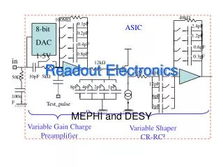
Conceptual design I basic preamp design, recommended by Photonique Hall D Electronics Meeting, Newport News, Oct. 23-24, 2007
Conceptual design II Embedded ethernet technology provides cheap and flexible communications bus FPGA provides interface 16-channel DAC provides Vbias Vbias readback using mulitplexed ADC temperature monitoring (for free) Hall D Electronics Meeting, Newport News, Oct. 23-24, 2007
Implementation • Xilinx FPGA • external components modeled in VHDL • detailed simulation during and after design using Xilinx development tools • robust set of test sequences to exercise major functions • ethernet complexity handled by ethernet controller – only host bus side simulated Hall D Electronics Meeting, Newport News, Oct. 23-24, 2007
Implementation Example: Addressing and initialization scheme Hall D Electronics Meeting, Newport News, Oct. 23-24, 2007
Project status and plans • Project started by 1 undergraduate student summer 2007 • Taken over fall 2007 by graduate student • VHDL design of digital side 70% finished • Single channel of preamp passed tests on bench • PADS PCB layout software PADS licenced installed at Uconn for layout • Design (analog+digital) expected to be ready for prototyping summer 2008 Hall D Electronics Meeting, Newport News, Oct. 23-24, 2007
