Lecture #22
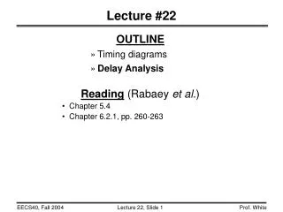
Lecture #22. OUTLINE Timing diagrams Delay Analysis Reading (Rabaey et al .) Chapter 5.4 Chapter 6.2.1, pp. 260-263. t pHL. t pLH. 1. F. t. 0. To further simplify timing analysis, we can define the propagation delay as. Propagation Delay in Timing Diagrams.

Lecture #22
E N D
Presentation Transcript
Lecture #22 OUTLINE • Timing diagrams • Delay Analysis Reading (Rabaey et al.) • Chapter 5.4 • Chapter 6.2.1, pp. 260-263
tpHL tpLH 1 F t 0 To further simplify timing analysis, we can define the propagation delay as Propagation Delay in Timing Diagrams • To simplify the drawing of timing diagrams, we can approximate the signal transitions to be abrupt (though in reality they are exponential). A F 1 A t 0
B 1 t 0 B•C 1 t 0 A+B 1 t 0 F 1 0 Glitching Transitions A,B,C The propagation delay from one logic gate to the next can cause spurious transitions, called glitches, to occur. (A node can exhibit multiple transitions before settling to the correct logic level.) 1 t 0 tp 2tp 3tp A+B A B F B C B•C t
Glitch Reduction • Spurious transitions can be minimized by balancing signal paths Example: F = A•B•C•D
MOSFET Layout and Cross-Section Top View: Cross Section:
Source and Drain Junction Capacitance Csource = Cj(AREA) + Cjsw(PERIMETER) = CjLSW + CJSW(2LS + W)
V DD Computing the Output Capacitance Example 5.4 (pp. 197-203) 2l=0.25mm Out In PMOS W/L=9l/2l Poly-Si Out In NMOS W/L=3l/2l GND Metal1
V DD 2l=0.25mm • Capacitances for 0.25mm technology: • Gate capacitances: • Cox(NMOS) = Cox(PMOS) = 6 fF/mm2 • Overlap capacitances: • CGDO(NMOS) = Con = 0.31fF/mm • CGDO(PMOS)= Cop = 0.27fF/mm • Bottom junction capacitances: • CJ(NMOS) = KeqbpnCj = 2 fF/mm2 • CJ(PMOS) = KeqbppCj = 1.9 fF/mm2 • Sidewall junction capacitances: • CJSW(NMOS) = KeqswnCj = 0.28fF/mm • CJSW(PMOS) = KeqbppCj = 0.22fF/mm PMOS W/L=9l/2l Out In NMOS W/L=3l/2l GND
Typical MOSFET Parameter Values • For a given MOSFET fabrication process technology, the following parameters are known: • VT (~0.5 V) • Coxand k (<0.001 A/V2) • VDSAT ( 1 V) • l ( 0.1 V-1) Example Req values for 0.25 mm technology (W = L):
Examples of Propagation Delay • Typical clock periods: • high-performance mP: ~15 FO4 delays • PlayStation 2: 60 FO4 delays
V DD MP1 v out CL + v in - MN1 STATIC CMOS DRIVING LARGE LOADS The load, CL , may be the capacitance of a long line on the chip (e.g. up to 1pF, or may be the load on one of the chip output pins (e.g. up to 50pF). We have seen that the typical driving resistance R for a minimum sized inverter is in the range of 10 KW. A 1 KW resistor driving a 50pF load would have a stage delay of 35nsec, huge in comparison to normal stage delays. Thus we need to use larger devices to drive large capacitive loads, that is greatly increase W/L. However, increasing W/L of a stage will increase the load it presents to the stage driving it, and we just move the delay problem back one stage.
V V DD DD MPB MP1 v out PROPOSED SOLUTION: Insert several simple inverter stages with increasing W/L between Inverter 1 + v in - MNB MN1 and the load CL. The total delay through the multiple stages will be less than the delay of one single stage driving CL. V DD MPB2 MPB1 MPB3 MP1 v out CL + v in - MNB2 MNB1 MNB3 MN1 STATIC CMOS DRIVING LARGE LOADS PROBLEM: A minimum sized inverter drives a large load, CL, leading to excessive delay, even with a buffer stage. CL
STATIC CMOS DRIVING LARGE LOADS V DD MPB MP1 v out + v in 50 pF - MNB MN1 W/L = 4 W/L = 9615 Example: The 2.5V 0.25mm CMOS inverter driving 50 pF load. Properties:W/L|N =1/.25, W/L|P =2/.25, VDD = 2.5V, VT = 0.5V. Rn = 13 KW /4 = 3.25 KW ; Rp = 31 KW /8 = 3.75 KW 5nm oxide thickness , Cox =6.9 fF/mm2. NMOS: CGp = W x L x Cox =1.7fF. PMOS : CGp = W x L x Cox =3.4fF. Thus CIN= 5.2fF Basic gate delay (0.69RC) is about 10pS. If we size one inverter to drive the load with this time constant it requires a W/L increase by a factor of 50pF/5.2fF =9615. So CIN= 50000fF =50pF for the buffer gate! Thus the gate delay for the first stage is (50000/5.2)X10pS = 96.1nS. Total delay = 96.1 + .01 = 96.11nS. TOO LONG and NO IMPROVEMENT! Note: We are ignoring drain capacitance in these examples.
V DD MPB2 MPB1 MPB3 MP1 v out CL + v in - MNB2 MNB1 MNB3 MN1 STATIC CMOS DRIVING LARGE LOADS Same example with tapered device sizes (geometric series) Case 1: Same example, but with buffer devices scaled by factor of 98 (982=9615 ) Stage 1 load = 98 X 5.2fF, (R= 3.5K) Stage 2 load = 50 pF , (R = 3.5K /98) Delay = 98 X 10pS + 96nS/98 =0.98 +0.98 nS ~2nS Case 2: Now taper through 3 buffer stages with W/L ratios of 9.9 (9.94=9615) 4 equal gate delays of 9.9 x 10pS =99pS Total = 4 X .099nS ~0.4nS Gate delay through 4 gates is much less than through 2! Note: We are ignoring drain capacitance in these examples.
V DD MPB2 MPB1 MPB3 MP1 v out CL + v in - MNB2 MNB1 MNB3 MN1 STATIC CMOS DRIVING LARGE LOADS Comments In our example we got better results with 3 buffer stages than 1. 7 buffer stages would do even better. How many buffer stages are optimum? Well under these simple assumptions (like ignoring drain and wiring capacitance, and operating asynchronously) you can show that the number of buffer stages, N obeys N +1 = ln(R) where R is the ratio of the load capacitance to the capacitance of a minimum sized stage. This formula is not important, but you should remember the concept that buffering with multiple stages usually leads to lower net delay if the load is large.

