Download
1 / 72
760 likes | 1.48k Vues
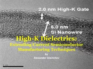
ECSE-6290 Semiconductor Devices and Models II Lecture 16: HBTs. Prof. Shayla M. Sawyer Bldg. CII, Room 8225 Rensselaer Polytechnic Institute Troy, NY 12180-3590 Tel. (518)276-2164 FAX (518)276-2990 e-mail: ssawyer@ecse.rpi.edu. HBT Lecture Outline. Introduction to HBTs

E N D
ECSE-6290Semiconductor Devices and Models IILecture 16: HBTs Prof. Shayla M. Sawyer Bldg. CII, Room 8225 Rensselaer Polytechnic Institute Troy, NY 12180-3590 Tel. (518)276-2164 FAX (518)276-2990 e-mail: ssawyer@ecse.rpi.edu
HBT Lecture Outline • Introduction to HBTs • Comparisons and Applications • Principle of Operation • Material Systems • Device Structures • Summary
Introduction “The HBT is an area of great industrial importance. It is no exaggeration to say that the entire cell phone industry depends on the HBT" From Peter Asbeck’s election article announcement into the National Academy of Engineering (NAE) pioneer of HBT technology Prediction by Shockley and Kroemer in late 1950s
Introduction KOPIN: First company to commercialize volume production of GaAs HBT (1996) High frequency operation =more data to be transmitted through a fiber or wireless system Linearity (signal quality) = ensures clear, reliable transmission of voice and data. Efficiency (power consumption) = extend the talk-time or data transmit time due to their lower power consumption Robustness (breakdown) = high breakdown handles voltage swings in the handset Simpler Design (small battery) = components, use of one low-voltage battery means ultra-thin cell phones
Introduction • Advantages of HBT • High fmax and fT • High power density • High breakdown voltage • High power handling capability • Good linearity • High transconductance • Low 1/f noise • Low base spreading resistance • High electron mobility (ballistic and overshoot effects) • Can be integrated with HEMTs, MESFETs and Schottky Diodes
Introduction Short answer for further discussion: • Wide band gap emitter • Higher base doping concentration • Very thin base layer • Base transit time reduced • Early voltage increased • Lower emitter doping • Semi-insulating substrate • Other device structure variations
Comparisons and Applications • High transconductance allows greater current handling capabilities than FETs • Voltage threshold for current flow is controlled by the built-in base-emitter junction • Good for manufacturing • Very uniform and reproducible device characteristics http://www.postech.ac.kr/ee/mmic/RFdevice/comp.html
Principle of Operation • Wide bandgap emitter • Dependence of common-emitter current gain on doping levels and energy band discontinuity at the emitter-base interface • Exponent factor can be very large to compensate for Nde/Nbe ratio
Principle of Operation • Spike • Conduction band discontinuity impedes electron current flow • Potential barrier for electron entering base from emitter region • Kroemer 1982 electron enters base with very large kinetic energies (close to ΔEc) which means high velocities (up to several times 105 m/s) • “Hot” electrons may reduce transit time and increase HBT cutoff frequency • Notch • Collects electrons at base which may increase recombination losses Spike-Notch e- How do you reduce the spike-notch?
Principle of Operation • Two main uses of grading (varying composition over distance) • Reduce spike for better emitter base electron current conduction • Grade the base for quasi-field to assist with the drift of electrons • High electron current and current gain • Reduced base charging time for higher fT • Increased Early voltage • Often used with SiGe a) Abrupt HBT b) Graded HBT c) Graded DHBT d) Graded-base bipolar transistor
Principle of Operation • Base doping higher than emitter doping • Lower base resistance improves fmax • Scaling limitation due to punch through eliminated • Base charge is insensitive to output voltage VCB (Early voltage increases ) • Reduced high current effects
Principle of Operation • Lower emitter doping • Reduced bandgap narrowing • Reduction in minority carrier concentration in the emitter • Improvement in current gain • Reduced CBE • Emitter-base space-charge region broadens on emitter side of the junction Reduction in emitter doping levels reduces what? Why?
Principle of Operation • Double Heterojunction Bipolar Transistor • Create another heterojunction at the base-collector • Eliminates injection of holes from the base into the collector when base-collector becomes forward biased • Diminishes saturation stored-charge density and speeds up device turn off • Increase in breakdown voltage • Reduction in leakage current
Material Systems: AlGaAs/GaAs • Lattice match is beneficial • Difference in lattice constant between AlAs and GaAs is on the order of 0.14% at room temperature • Significant bandgap differences can be obtained • Abrupt Np heterojunction have significant conduction band energy barriers • Electron and hole mobility 8000 cm2/V-s and 380 cm2/V-s repectively (free of impurity scattering) • Semi-insulating substrate (isolate devices and interconnects)
Material Systems: AlGaAs/GaAs Single Heterojunction abrupt HBT • Output conductance • High positive output resistance or differential negative output resistance • High doping of base region • Base Gummel number is not significantly changed with B-C bias • Early Voltage in the range of 100 to 200 V
Material Systems: AlGaAs/GaAs • Offset voltage • Voltage that must be applied before a positive Ic will flow • Turn on voltage for current flow in B-E junction is greater than that for B-C junction • Conduction band barrier mostly • Also hole flow in forward biased CB (doping ratio) • Use wide band gap collector to reduce
Material Systems: AlGaAs/GaAs • Current gain • Decreases to less than unity for very low Ic values • Base current arises from recombination at the B-E space charge region due to deep levels in the AlGaAs and GaAs • Recombination associated with emitter periphery
Material Systems: InGaAs/InP • High electron mobility in InGaAs, (13,000 cm2/V-s) 1.6 times higher than GaAs and 9 times higher than Si (pure materials) • Transient electron velocity overshoot greater than GaAs • Bandgap is smaller than GaAs or Si, turn on VBE is smaller (with graded heterojuction) • Power supply voltage and power dissipation can be lower • Recombination velocity at surfaces is smaller than GaAs surfaces (103 rather than 106 cm/s) so its easier to scale • High substrate thermal conductivity than GaAs
Abrupt B-E Graded B-E Material Systems: InGaAs/InP • High current gain even with narrow emitters • High frequency performance fT among highest ~165 GHz • Overall advantages are scalability and ultra high speed Abrupt Single Heterojunction HBT
Material Systems :SiGe SiGe HBTs have the added advantage of monolithic integration into mature Silicon technology, (CMOS, VLSI) “Silicon-Germanium (SiGe) technology is the driving force behind the explosion in low-cost, lightweight, personal communications devices like digital wireless handsets, as well as other entertainment and information technologies like digital set-top boxes, Direct Broadcast Satellite (DBS), automobile collision avoidance systems, and personal digital assistants. “ http://www.eng.auburn.edu/~guofu/sige_intro.htm
Material Systems: SiGe • Addition of Ge reduces the bandgap of Si, leading to an alloy that can be used to form the base region of the HBT • Decrease in bandgap lead to changes in the IC-VBE relation toward lower turn on voltage • Lattice mismatch requires epitaxial layers to be grown below a critical thickness (pseudomorphic growth) • Strain provides benefits for transistor operation • Effective mass perpendicular to the heterojunction reduces 60% from unstrained case
Material Systems: SiGe Overcame issues with lattice matching IBM started technology for high end computing but refocused to the communications market SiGe HBTs consume much less power than CMOS for the same level of performance Integrated SiGe chips can be found in GSM and CDMA wireless handsets and base stations, wireless LAN chipsets, and high-speed 10-40 Gb/s synchronous optical network (SONET) transceivers.
Material Systems: SiGe http://www.eng.auburn.edu/~guofu/sige_intro.htm Ge composition is typically graded across the base to create an accelerating electric field for minority carriers moving across the base, typically 30-50 kV/cm A direct result of the Ge grading in the base is higher speed, and thus higher operating frequency.
Material Systems O. Esame, Y. Gurbuz, I. Tekin, A. Bozkurt, “Performance comparison of state-of-the-art heterojunction bipolar devices (HBTS) based on AlGaAs/GaAs, Si/SiGe and InGaAs/InP”, Microelectronics Journal, 35, p. 901-908, (2004). • SiGe based devices for low noise applications (low noise amplifiers) due to better noise behavior • GaAs based devices for high power applications due to higher breakdown voltages • InP based devices for high speed applications
Device Structures Collector-up structure Traditionally built with a larger collector than emitter for efficient collection, (better current gain) Smaller capacitor area gives smaller collector capacitance Reduction of lead inductance in series with the emitter Increases speed significantly
Device Structures: Tunneling Emitter Bipolar Transistor • Wide band gap AlGaAs is replaced by a conventional n+-GaAs emitter • Thin graded AlGaAs layer is inserted between emitter and base • Varying tunneling rates for electrons and holes (mass filtering) Schematic diagram of Tunneling Emitter Bipolar (TEBT) from Xu and Shur (1986)
Device Structures: Tunneling Emitter Bipolar Transistor Proposed Advantages: • Easier to fabricate • Smaller emitter contact resistance • High gain • Fewer traps Schematic diagram of Tunneling Emitter Bipolar (TEBT) from Xu and Shur (1986)
Example Problem A HBT has a bandgap of 1.62 eV for the emitter and 1.42 eV for the base. A homojunction BJT has a bandgap of 1.42 eV for both the emitter and the base; it has an emitter doping of 1018 cm-3 and a base doping of 1015 cm-3. If the HBT has the same emitter doping and the same common-emitter current gain β0 as the BJT, what is the lower bound of the base doping of the HBT (in atoms/cm3)? Assume: Base transport factor is close to unity β0 is mainly determined by emitter efficiency Diffusion constant, densities of states in conduction band and valence band are the same for emitter and base Neutral base width W is much less than the base diffusion length and is = or < emitter diffusion length
Summary • HBTs are a major contributor to the cell phone industry • Wide band gap emitter allows for compensation for low doping ratio • Grading is often used to reduce the “spike” and create a quasi field that increases fT • High base doping, lower emitter doping improves performance • Double Heterojunction (wide band gap collector) reduces offset voltage, increases break down voltage, and reduces leakage current • Material systems AlGaAs/GaAs, InGaAs/InP, and SiGe are often used
ECSE-6290Semiconductor Devices and Models IILecture 17: HBT Models Prof. Shayla M. Sawyer Bldg. CII, Room 8225 Rensselaer Polytechnic Institute Troy, NY 12180-3590 Tel. (518)276-2164 FAX (518)276-2990 e-mail: ssawyer@ecse.rpi.edu
HBT Advantage Review • Because of alignment of band edges • The injection charge from base to emitter is greatly suppressed • Nearly unity injection efficiencies • High current gains • No longer rely on ratio of emitter to base doping levels to suppress injection from base to emitter • Increase base doping and decrease emitter doping • Smaller base spreading resistance • Lower emitter to base capacitance
HBT Lecture Outline Book Reference: Semiconductor Device Modeling for VLSIby Kwyro Lee, Michael Shur, Tor. A. Fjeldly, and Trond Ytterdal, Prentice Hall, (1993). • Modeling • Thermionic Emission Diffusion • Thermionic Field Emission Diffusion • Thermionic Field Diffusion (for graded emitter) • Fabrication • Scaling • Summary
Modeling • Discontinuity in conduction band edge at E-B interfaces gives rise to barrier impeding injection of electrons into base region • Anderson (1962) thermionic model • Grinberg (1984) accounting for tunneling near the top of the barrier • Lauterbach (1992) included other important factors (recombination current, emitter series resistance etc. Barrier height at x=-WGR Voltage drop across depletion region on base side Voltage drop across depletion region on emitter side boundary of space charge region on emitter and base side of EB junction boundary of space charge region on base side of BC junction
Modeling Common emitter current gain β as a function of collector current for the abrupt heterojunction for different base doping levels with respect to a emitter doping level of 2*1017 cm-3 The increase due to tunneling is about a factor of ten for the abrupt junction A. Grinberg, M. Shur, R. Fischer, and H. Morkoc, IEEE Transactions on Electron Devices, vol. ED-31, pg. 1758, (1984).
Modeling • Remember: Ebers Moll Model for the BJT • Intrinsic emitter and collector currents in terms of pn diode currents • HBT models are accounting for how carriers traverse the discontinuity in the conduction band
Modeling • Electron Current Density at EB junction • J’n(x=0) = J’n(xb) (space charge region at EB junction) • Includes excess electron concentration contribution from collector at base side of the boundary • Hole Current Density at EB junction • J’P(-xe) • Electron Current Density at BC junction • J’n(x’b) • Hole Current Density at BC junction • J’P(xc) Barrier height at x=-WGR Voltage drop across depletion region on base side Voltage drop across depletion region on emitter side boundary of space charge region on emitter and base side of EB junction boundary of space charge region on base side of BC junction
Modeling: Thermionic Emission Diffusion Model • Electron current density across heterojunction for emitter-base interface • x=0 is the position of the heterointerface, • Jeb and Jbe are the current densities associated with the flux of electrons from the emitter to base and vice versa • vn mean thermal velocity in the x-direction • n(0-) and n(0+) are the electron concentrations at the emitter and base side of the heterointerface
Modeling: Thermionic Emission Diffusion Model • These electron concentrations related to those at the boundaries of the emitter base regions, x=-xe and x=xb Vbieb is the built in potential Vbe is the applied forward biased voltage Nab doping levels in the base Nde doping levels in emitter
Modeling: Thermionic Emission Diffusion Model • Electron current density is equal to the electron current density due to diffusion at the boundary of the space charge region in the base (neglecting interface recombination) expressed as • The excess electron concentration at the base side boundary of the base-emitter depletion region n(x b)-nbo
Modeling: Thermionic Emission Diffusion Model • The excess electron concentration at the base side boundary of the base-emitter depletion region n(x b)-nbo Collector side contribution Emitter side contribution • Typically in HBTs the base is highly doped • ΔEn is the additional energy barrier for electrons entering from the emitter into the neutral base • Vdb is small so that qVdb<ΔEc and ΔEn>0 conduction band discontinuity creates an additional barrier for the electron entering the neutral section of the base region • When ΔEn<0 the conduction band spike is below the bottom of the conduction band in the neutral section of the base
Modeling: Thermionic Emission Diffusion Model • Using the following relationships, when ΔEn<0 (no discontinuity) • Nde is the equilibrium concentration in the emitter • Vbc is the base collector voltage nbo equilibrium concentration Jne is the electron current density with base shortened to the emitter and base collector junction reverse biased
Modeling: Thermionic Emission Diffusion Model • Assuming there is no spike in the valence band at the emitter base heterointerface, the hole component of the current density of emitter base interface can be treated like the conventional BJT • XE is the width of the neutral part of the emitter region and Effect of the band gap discontinuity will enter only through the equilibrium minority carrier concentration, peo
Modeling: Thermionic Emission Diffusion Model • Based on the diffusion model for the base region, find the following expression for the electron currentdensity on the base side edge of the base collector region
Modeling: Thermionic Emission Diffusion Model • The expression for thehole component of the current density of base collector interfacecan be treated like the conventional BJT pco equilibrium hole concentration in the collector XC width of the neutral part of the collector
Modeling: Thermionic Emission Diffusion Model • Having solved for the current components at each junction, the equations for intrinsic emitter and collector current densities can be written like Ebers-Moll equations for a homojunction BJT where
Modeling: Thermionic Emission Diffusion Model • Multiplying J’e and J’c with the base cross section S and rearranging, the intrinsic emitter and collector currents are Inverse common-base current gain Common-base collector reverse saturation current Normal forward current gain Emitter reverse saturation current
Modeling: Thermionic Emission Diffusion Model • In a typical device, Lnb>>WB, Lpe>>Xe, Lpc>>XC and ΔEn>>qVth • This allows the coefficients of the Ebers-Moll equations to be simplified Important for grading variation