Download
1 / 93
1.03k likes | 1.65k Vues
130nm and 90nm ASIC Technologies for SLHC applications at CERN . Ecole IN2P3 de microélectronique 2009 . Kostas Kloukinas CERN, PH-ESE dept. CH1211, Geneve 23 Switzerland. Microchips for Megastructures. Support of microelectronic technologies for SLHC upgrades.

E N D
130nm and 90nm ASIC Technologies for SLHC applications at CERN • Ecole IN2P3 de microélectronique 2009 Kostas Kloukinas CERN, PH-ESE dept. CH1211, Geneve 23 Switzerland
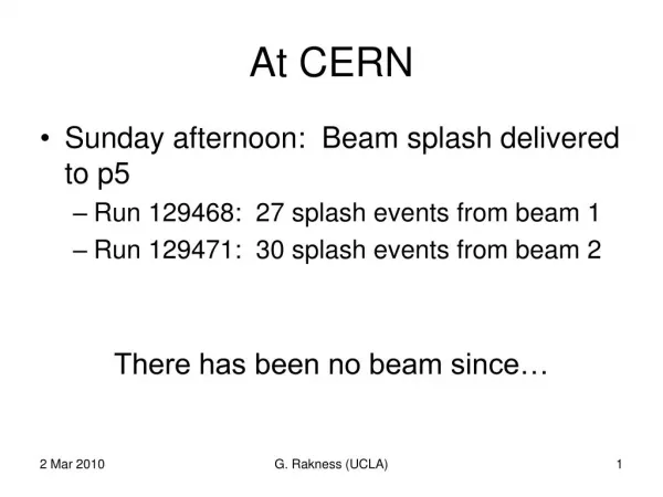
Microchips for Megastructures • Support of microelectronic technologies for SLHC upgrades. CMS experiment in the LHC accelerator at CERN Front-End ASIC Silicon Tracker Hybrid Kostas.Kloukinas@cern.ch
Overview • 130nm and 90nm Technologies • 130nm Mixed Signal Design Kit & Methodologies • Digital Block Implementation flow • Access to Foundry Services Kostas.Kloukinas@cern.ch
Overview of Technologies • Access to Foundry services & Technology technical support. • 130nm (CMOS & BiCMOS) and 90nm contract available since 6/2007. • Future technologies can be negotiated with the same manufacturer, once the necessity arise. CMOS 8RF-LM Low cost technology for Large Digital designs CMOS 8RF-DM Low cost technology for Analog & RF designs BiCMOS 8WLCost effective technology for Low Power RF designs BiCMOS 8HP High Performance technology for demanding RF designs CMOS 9SF LP/RF High performance technology for dense designs 130nm CMOS 90nm CMOS Kostas.Kloukinas@cern.ch
CMOS8RF 130nm technology Kostas.Kloukinas@cern.ch
CMOS8RF Technology Features Kostas.Kloukinas@cern.ch
Process cross-section (DM) Kostas.Kloukinas@cern.ch
Last metal options Kostas.Kloukinas@cern.ch
BEOL metallization options Supported by MOSIS Dominant choise Kostas.Kloukinas@cern.ch
CMOS8RF Devices Kostas.Kloukinas@cern.ch
FET devices Kostas.Kloukinas@cern.ch
FET Device options Kostas.Kloukinas@cern.ch
FET Device options T3 Isolation Well(New feature. Will be fully qualified with the release of the PDK V1.7, Dec.2009) Enables placement of both NFETs and PFETs in a well isolated form the bulk substrate. Additional mask level: T3. Zero-Vt devices are not allowed. Kostas.Kloukinas@cern.ch
Isolation Structures Kostas.Kloukinas@cern.ch
Metal-to-metal Capacitors (mimcap) Kostas.Kloukinas@cern.ch
Dual metal-to-metal Capacitors (dual mimcap) Kostas.Kloukinas@cern.ch
MOS Capacitors (ncap, dgncap) Kostas.Kloukinas@cern.ch
Vertical natural capacitor (vncap) Kostas.Kloukinas@cern.ch
Resistors Kostas.Kloukinas@cern.ch
Transmission Lines Kostas.Kloukinas@cern.ch
Coplanar Waveguide Kostas.Kloukinas@cern.ch
Electronic Fuse (eFuse) Kostas.Kloukinas@cern.ch
ESD Protection Strategy (1/2) Kostas.Kloukinas@cern.ch
ESD Protection Strategy (2/2) Kostas.Kloukinas@cern.ch
Design For Manufacturability • Floating Gates, Antenna ratios and Tie downs • Nwell and Triple well charging Kostas.Kloukinas@cern.ch
Pattern Density Rules • The cause of many design Tape Out delays! • Early consideration of pattern density rules is essential. • The Foudry will autofill RX, PC, M1, M2, M3, MQ and MG; The designer should not attempt to fill any of these layers himself. • The Foundry will NOT autofill the "RF-metals" LY, E1 and MA. The designer must meet all global,andlocal, rules for all three RF-metals. Kostas.Kloukinas@cern.ch
CMOS8WL (SiGe) 130nm technology Kostas.Kloukinas@cern.ch
BiCMOS (SiGe) 130nm Kostas.Kloukinas@cern.ch
CMOS8WL vs. CMOS8RF Kostas.Kloukinas@cern.ch
CMOS9LP/RF 90nm technology Kostas.Kloukinas@cern.ch
90nm Technology Features Kostas.Kloukinas@cern.ch
CMOS9 technology derivatives • CMOS 9SF • Core/IO Voltage: 1.0V/2.5V • Ideal for leading-edge microprocessors, communications, and computer data processing applications. • CMOS 9LP/RF • Core/IO Voltage: 1.2V/2.5V • Use for low-cost, high performance wireless applications, as Bluetooth, WLAN, cellular handsets, mobile TV, WiMax, UWB and GPS. • THIS IS THE TECHNOLOGY OF OUR CHOISE • MPW service support Kostas.Kloukinas@cern.ch
CMOS9LP/RF devices • CMS9FLP/RF offers up to eight NFETs. Six of these (all but the Zero-VT FETs) are available with either dual well or triple well construction. • An optional set of FET pcells is provided for RF applications Kostas.Kloukinas@cern.ch
Process Cross-sections One Aluminum pad metal Up to 1, 12x-pitch metal on thick oxide Up to 2, 2x-pitch metals on thick oxide Up to 6, 1x-pitch metals on low-K dielectric • MPW service supported metal stack • 8 metal stack (M1, M2, M3, M4, M5, M1_2B, OL and LD top-metal to DV (glass cut) Kostas.Kloukinas@cern.ch
Technology support at CERN • Foundry PDK V1.4 currently available. • Distributed to a small number of institutes. • Future Plans: • Investigate options for a digital standard cell library. • Develop a mixed-signal design kit that supports the same design workflows as for the CMOS8RF. Kostas.Kloukinas@cern.ch
CMOS8RF Analog & Mixed Signal Design Kostas.Kloukinas@cern.ch
Challenges • Technology • Complex physical design rules and Manufacturability constrains. • Multiple corners for design simulations. • Tough Signal Integrity issues, and difficult final Timing Closure. • Expensive prototyping. • CAE Tools • Multiplicity of tools and complicated - non linear - design flows. • Numerous data formats used when interfacing tools from different tool vendors. • Designs • Demanding Power analysis and power management. • Chip level integration and assembly. • Large chips require to extend design efforts to multiple teams across geographically distributed institutes. Kloukinas Kostas CERN
Requirements • Formalize the methodologies in our design environment. • Allow designers of the HEP community to become familiar with complex tools, necessary to master large designs in a modern technology. • Assist digital design with an automated workflow. • Common design platform across multiple institutes. • Enhance team productivity. • Provide a silicon accurate methodology. • Increase silicon reliability. Kloukinas Kostas CERN
Objectives • Development of: • “Mixed Signal Design Kit” • “Analog & Mixed Signal Methodologies (Workflows)” • Provide: • Maintenance • Training • Support Kostas.Kloukinas@cern.ch
Typical ASIC designs at CERN • Typical ASIC designs: • Analog circuits with complex full custom designs • Mixed Signal with large high performance analog and small digital circuits • Digital circuits not exceeding 300K gates. 128ch pre-amp, analog memory chipset 4ch 40Msps 12-bit ADC 4ch data readout chip Gigabit Optical Link MEDIPIX1 Pixel chip Rad-Tol FPGA Kostas.Kloukinas@cern.ch
Mixed Signal Design kit • Objectives • Development of a “Design Kit” for Mixed Signal environments. • With integrated standard cell libraries. • Establish well defined Analog & Mixed Signal design workflows. • Targeted to big “A” (analog), small “D” (digital) ASICs. • Implemented on modern versions of CAE Tools. • Replace our previous Design Kit distribution. • Based on the ARM/ARTISAN cells and an automated digital only design flow. • Making use of old versions of CAE tools. • Two years in service. • Already distributed to 25 institutes • Users can continue using the old design kit and the ARM libraries since they have signed NDAs directly with ARM.Maintenance and technical support will be provided by ARM. MR Design kit Kostas.Kloukinas@cern.ch
Mixed Signal design kit • Key Features: • PDK V1.6 • Foundry Standard cell and IO pad libraries • Physical Layout views available. • Separate substrate contacts for mixed signal low noise applications. • Access to standard cells libraries is legally covered by already established Foundry CDAs • New versions of CAE Tools • Open Access database support for increased interoperability of Virtuoso and SOC-Encounter environments. • Compatible with the “Europractice” distributions. • Support for LINUX Platform (qualified on RHEL4) PDK Standard cell libraries CAE Tools Mixed Signal Design Kit • Two independent design kits: • CMOS8RF-LM (6-2 BEOL) • CMOS8RF-DM (3-2-3 BEOL) Kostas.Kloukinas@cern.ch
CMOS8RF Core Library Standard Cell Primitive Logic AND2 2-Way AND AND3 3-Way AND AND4 4-Way AND INVERT Inverter INVERTBAL Balanced Inverter NAND2 2-Way NAND NAND2BAL Balanced 2-Way NAND NAND3 3-Way NAND NAND4 4-Way NAND NOR2 2-Way NOR NOR3 3-Way NOR NOR4 4-Way NOR OR2 2-Way OR OR3 3-Way OR OR4 4-Way OR XOR2 2-Way XOR XOR3 3-Way XOR XOR8 8-Way XOR (8-Bit Parity Odd) XOR9 9-Way XOR (9-Bit Parity Odd) XNOR2 2-Way XNOR XNOR3 3-Way XNOR Standard Cell Complex Logic AO21 2x1 AND OR AO22 2x2 AND OR AO33 3x3 AND OR AO44 4x4 AND OR AO222 2x2x2 AND OR AO2222 2x2x2x2 AND OR AOI21 2x1 AND OR Invert AOI22 2x2 AND OR Invert AOI33 3x3 AND OR Invert AOI44 4x4 AND OR Invert AOI222 2x2x2 AND OR Invert AOI2222 2x2x2x2 AND OR Invert OA21 2x1 OR AND OA22 2x2 OR AND OA222 2x2x2 OR AND OA2222 2x2x2x2 OR OAI21 2x1 OR AND Invert OAI22 2x2 OR AND Invert OAI222 2x2x2 OR AND Invert OAI2222 2x2x2x2 OR AND Invert Standard Cell Unique Logic ADDF Full Adder BUFFER Buffer CLK Clock Driver CLKI Inverting Clock Driver COMP2 2-Bit Comparator DECAP VDD–GND Decoupling Capacitor DELAY4 Delay Line DELAY6 Delay Line MUX21 2:1 Multiplexer MUX21BAL Balanced 2:1 Multiplexer MUX21I 2:1 Multiplexer w/Inverted Output MUX41 4:1 Multiplexer TERM Net Terminator Standard Cell Sequential Latches DFF D Flip-Flop, Q and QBAR Outputs. DFFR D Flip-Flop, Q and QBAR Outputs, -Asyn Reset DFFS D Flip-Flop, Q and QBAR Outputs, Asyn Set DFFSR D Flip-Flop, Q and QBAR Outputs, Asyn Set, -Asyn Reset LATSR Latch w/Q and QBAR Outputs, Asyn Set, -Asyn Reset SDFF Scannable D Flip-Flop, Q and QBAR Outputs SDFFR Scannable D Flip-Flop, Q and QBAR Outputs, -Asyn Reset SDFFS Scannable D Flip-Flop, Q and QBAR Outputs, Asyn Set SDFFSR Scannable D Flip-Flop, Q and QBAR Outputs, Asyn Set, -Asyn Reset SLATSR Scannable Latch w/Q and QBAR Outputs, Asyn Set, -Asyn Reset Physical Design Cells FILL1, FILL2 One and Two Cell Post-Fill Cells FGTIE_G Floating Gate Tie-Off GAUNUSEDxxx Gate Array Post-Fill Cells NWSX N-Well/Substrate Tie-Off Cell 7 driving strength derivatives / cell Kostas.Kloukinas@cern.ch
CMOS8RF IO pad Library Standard Cell I/Os BC1520, BC1520_PM 1.5 V CMOS Nontest 20 Ohm 3-State I/O BC1535, BC1535_PM 1.5 V CMOS Nontest 35 Ohm 3-State I/O BC1550, BC1550_PM 1.5 V CMOS Nontest 50 Ohm 3-State I/O BC1565, BC1565_PM 1.5 V CMOS Nontest 65 Ohm 3-State I/O BC1590, BC1590_PM 1.5 V CMOS Nontest 90 Ohm 3-State I/O BC1520PD, BC1520PD_PM 1.5 V CMOS Nontest 20 Ohm 3-State I/O w/Pull-Down BC1535PD, BC1535PD_PM 1.5 V CMOS Nontest 35 Ohm 3-State I/O w/Pull-Down BC1550PD, BC1550PD_PM 1.5 V CMOS Nontest 50 Ohm 3-State I/O w/Pull-Down BC1565PD, BC1565PD_PM 1.5 V CMOS Nontest 65 Ohm 3-State I/O w/Pull-Down BC1590PD, BC1590PD_PM 1.5 V CMOS Nontest 90 Ohm 3-State I/O w/Pull-Down BC1520PU, BC1520PU_PM 1.5 V CMOS Nontest 20 Ohm 3-State I/O w/Pull-Up BC1535PU, BC1535PU_PM 1.5 V CMOS Nontest 35 Ohm 3-State I/O w/Pull-Up BC1550PU, BC1550PU_PM 1.5 V CMOS Nontest 50 Ohm 3-State I/O w/Pull-Up BC1565PU, BC1565PU_PM 1.5 V CMOS Nontest 65 Ohm 3-State I/O w/Pull-Up BC1590PU, BC1590PU_PM 1.5 V CMOS Nontest 90 Ohm 3-State I/O w/Pull-Up BC1820, BC1820_PM 1.8 V CMOS Nontest 20 Ohm 3-State I/O BC1835, BC1835_PM 1.8 V CMOS Nontest 35 Ohm 3-State I/O BC1850, BC1850_PM 1.8 V CMOS Nontest 50 Ohm 3-State I/O BC1865, BC1865_PM 1.8 V CMOS Nontest 65 Ohm 3-State I/O BC1820PD, BC1820PD_PM 1.8 V CMOS Nontest 20 Ohm 3-State I/O w/Pull-Down BC1835PD, BC1835PD_PM 1.8 V CMOS Nontest 35 Ohm 3-State I/O w/Pull-Down BC1850PD, BC1850PD_PM 1.8 V CMOS Nontest 50 Ohm 3-State I/O w/Pull-Down BC1865PD, BC1865PD_PM 1.8 V CMOS Nontest 65 Ohm 3-State I/O w/Pull-Down BC1820PU, BC1820PU_PM 1.8 V CMOS Nontest 20 Ohm 3-State I/O w/Pull-Up BC1835PU, BC1835PU_PM 1.8 V CMOS Nontest 35 Ohm 3-State I/O w/Pull-Up BC1850PU, BC1850PU_PM 1.8 V CMOS Nontest 50 Ohm 3-State I/O w/Pull-Up BC1865PU, BC1865PU_PM 1.8 V CMOS Nontest 65 Ohm 3-State I/O w/Pull-Up BC2520, BC2520_PM 2.5 V CMOS Nontest 20 Ohm 3-State I/O BC2535, BC2535_PM 2.5 V CMOS Nontest 35 Ohm 3-State I/O BC2550, BC2550_PM 2.5 V CMOS Nontest 50 Ohm 3-State I/O BC2565, BC2565_PM 2.5 V CMOS Nontest 65 Ohm 3-State I/O BC2590, BC2590_PM 2.5 V CMOS Nontest 90 Ohm 3-State I/O BC2520PD, BC2520PD_PM 2.5 V CMOS Nontest 20 Ohm 3-State I/O w/Pull-Down BC2535PD, BC2535PD_PM 2.5 V CMOS Nontest 35 Ohm 3-State I/O w/Pull-Down BC2550PD, BC2550PD_PM 2.5 V CMOS Nontest 50 Ohm 3-State I/O w/Pull-Down BC2565PD, BC2565PD_PM 2.5 V CMOS Nontest 65 Ohm 3-State I/O w/Pull-Down BC2590PD, BC2590PD_PM 2.5 V CMOS Nontest 90 Ohm 3-State I/O w/Pull-Down BC2520PU, BC2520PU_PM 2.5 V CMOS Nontest 20 Ohm 3-State I/O w/Pull-Up BC2535PU, BC2535PU_PM 2.5 V CMOS Nontest 35 Ohm 3-State I/O w/Pull-Up BC2550PU, BC2550PU_PM 2.5 V CMOS Nontest 50 Ohm 3-State I/O w/Pull-Up BC2565PU, BC2565PU_PM 2.5 V CMOS Nontest 65 Ohm 3-State I/O w/Pull-Up BC2590PU, BC2590PU_PM 2.5 V CMOS Nontest 90 Ohm 3-State I/O w/Pull-Up Standard Cell C4 I/Os for LM (BEOL) option Standard Cell Power Supply pads Kostas.Kloukinas@cern.ch
CMOS8RF Mixed Signal Workflows • Analog & Mixed Signal (AMS) Workflows. • Standardized, validated Design Workflows • Top-down design Partitioning. • Digital Block implementation flow • Mixed-Signal Simulation & design Concept Validation • Hierarchical design Floorplaning and Physical Assembly • Design Performance Validation and Physical Verification • CERN – VCAD Cadence -Foundrycollaboration • VCAD brought in their invaluable expertise on the CAE tools • Foundryprovided the physical IP blocks and important technical assistance. • CERN assists the development and validates the design kit functionality Kostas.Kloukinas@cern.ch
Analog & Mixed Signal Flows • Analog Driven (Analog on Top) design workflow • Top-Down Functional DesignEarly chip level verification strategy has to be in place and validated with correct partitioning between analog and digital. As the project is proceeding toward completion, the same top-level validation is done by replacing the behavioural model with a transistor-level description (including RC parasitic if required). • Top-Down Physical DesignEarly floorplanning (including pad placement) even with rough estimation of block (area, aspect ratio, pin location) will enable to plan for special nets routing (buses, clocks, power network, sensitive nets ...). As the project is proceeding toward completion, the same floorplanning could be refined and adapted. • Bottom-up Block Function& Physical DesignAnalog and Digital block circuit level implementation (transistors & gates) The Concept The use of the workflows may vary depending on the design requirements and organization of design teams. Kostas.Kloukinas@cern.ch
CAE Design Tools • Workflows are based mainly on Cadence tools • All versions are compatible with the Europractice 2008-2009 distribution Kostas Kloukinas CERN
Design Kit Distribution • The Design kit will be made available to collaborating institutes. • No access fees required. • Pay-per-use scheme. • Prototyping should be done through CERN • A small fee will be applied. • This should cover part of the design kit maintenance costs in the long term. • Planned for release in October 2009. • Announcement by e-mail to the “130nm user list”. • Acquiring the CMOS8RF Mixed Signal Design Kit • Contact Bert.Van.Koningsveld@cern.ch or Kostas.Kloukinas@cern.ch • Establish a CDA with Foundry (if not already in place). • Granted access to the CERN ASIC support web site. Kostas.Kloukinas@cern.ch
The CERN ASIC support website http://cern.ch/asic-support Download Design Kits and access technical documents (restricted access) Information about MPW runs and foundry access services. Communicate news and User support feedback forms and access request forms. This website replaces our ‘afs’ based download facility. Kostas.Kloukinas@cern.ch
User Support and Training • Maintenance • Distribution of: • PDK updates. • Design Flow updates and enhancements. • Updates to accommodate new releases of CAE tools. • User Support • Limited to the distributed Design Kit version, under the supported versions of the CAE design tools. • Training sessions • Scheduled sessions: • 1st session: 26 to 30 October (CERN internal) • 2nd session: 16 to 20 November (open to external engineers) • 3rd session: 30 Nov to 4 December (outside CERN) Kostas.Kloukinas@cern.ch