Download
1 / 41
410 likes | 660 Vues
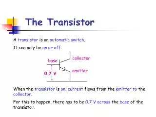
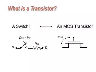
|V. |. GS. A Switch!. An MOS Transistor. What is a Transistor?. The MOS Transistor. Polysilicon. Aluminum. MOS Transistors - Types and Symbols. D. D. G. G. S. S. Depletion. NMOS. Enhancement. NMOS. D. D. G. G. B. S. S. NMOS with. PMOS. Enhancement. Bulk Contact.

E N D
|V | GS A Switch! An MOS Transistor What is a Transistor?
The MOS Transistor Polysilicon Aluminum
MOS Transistors -Types and Symbols D D G G S S Depletion NMOS Enhancement NMOS D D G G B S S NMOS with PMOS Enhancement Bulk Contact
-4 x 10 6 VGS= 2.5 V 5 Resistive Saturation 4 VGS= 2.0 V Quadratic Relationship (A) 3 VDS = VGS - VT D I 2 VGS= 1.5 V 1 VGS= 1.0 V 0 0 0.5 1 1.5 2 2.5 V (V) DS Current-Voltage RelationsA good ol’ transistor
Pinch-off Transistor in Saturation
-4 x 10 2.5 VGS= 2.5 V Early Saturation 2 VGS= 2.0 V 1.5 Linear Relationship (A) D I VGS= 1.5 V 1 VGS= 1.0 V 0.5 0 0 0.5 1 1.5 2 2.5 V (V) DS Current-Voltage RelationsThe Deep-Submicron Era
5 u = 10 sat ) s / m ( n u x = 1.5 x (V/µm) c Velocity Saturation Constant velocity Constant mobility (slope = µ)
Perspective I D Long-channel device V = V GS DD Short-channel device V V - V V DSAT GS T DS
-4 x 10 -4 x 10 6 2.5 5 2 4 1.5 (A) 3 (A) D D I I 1 2 0.5 1 0 0 0 0.5 1 1.5 2 2.5 0 0.5 1 1.5 2 2.5 V (V) V (V) GS GS ID versus VGS linear quadratic quadratic Long Channel Short Channel
-4 -4 x 10 x 10 2.5 6 VGS= 2.5 V VGS= 2.5 V 5 2 Resistive Saturation VGS= 2.0 V 4 VGS= 2.0 V 1.5 (A) (A) 3 D D VDS = VGS - VT I I VGS= 1.5 V 1 2 VGS= 1.5 V VGS= 1.0 V 0.5 1 VGS= 1.0 V 0 0 0 0.5 1 1.5 2 2.5 0 0.5 1 1.5 2 2.5 V (V) V (V) DS DS ID versus VDS Long Channel Short Channel
G S D B A unified modelfor manual analysis
-4 x 10 2.5 VDS=VDSAT 2 VelocitySaturated 1.5 Linear 1 VDSAT=VGT 0.5 VDS=VGT Saturated 0 0 0.5 1 1.5 2 2.5 Simple Model versus SPICE (A) D I V (V) DS
-4 x 10 0 -0.2 -0.4 (A) D I -0.6 -0.8 -1 -2.5 -2 -1.5 -1 -0.5 0 V (V) DS A PMOS Transistor VGS = -1.0V VGS = -1.5V VGS = -2.0V Assume all variables negative! VGS = -2.5V
Polysilicongate Source Drain W x x + + n n d d Gate-bulk L d overlap Top view Gate oxide t ox + + n n L Cross section The Gate Capacitance
Gate Capacitance Cut-off Resistive Saturation Most important regions in digital design: saturation and cut-off
Gate Capacitance Capacitance as a function of the degree of saturation Capacitance as a function of VGS (with VDS = 0)
Diffusion Capacitance Channel-stop implant N 1 A Side wall Source W N D Bottom x Side wall j Channel L Substrate N S A
Linearizing the Junction Capacitance Replace non-linear capacitance by large-signal equivalent linear capacitance which displaces equal charge over voltage swing of interest
The Sub-Micron MOS Transistor • Threshold Variations • Subthreshold Conduction • Parasitic Resistances
V V T T Threshold Variations Low V threshold Long-channel threshold DS VDS L Threshold as a function of Drain-induced barrier lowering the length (for low V ) (for low L ) DS
-2 10 Linear -4 10 -6 Quadratic 10 (A) D I -8 10 Exponential -10 10 VT -12 10 0 0.5 1 1.5 2 2.5 V (V) GS Sub-Threshold Conduction The Slope Factor S is DVGS for ID2/ID1 =10 Typical values for S: 60 .. 100 mV/decade
Sub-Threshold ID vs VGS VDS from 0 to 0.5V
Sub-Threshold ID vs VDS VGS from 0 to 0.3V
Summary of MOSFET Operating Regions • Strong Inversion VGS >VT • Linear (Resistive) VDS <VDSAT • Saturated (Constant Current) VDS VDSAT • Weak Inversion (Sub-Threshold) VGS VT • Exponential in VGS with linear VDS dependence
Future Perspectives 25 nm FINFET MOS transistor