Transistors
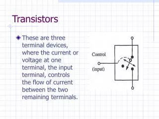
Transistors. Transistor Definitions. MOS - Metal Oxide Semiconductor FET - Field Effect Transistor BJT - Bipolar Junction Transistor. drain. collector. body. base. gate. source. emitter. npn bipolar transistor. n-channel MOSFET. MOSFET and BJT. Basic MOSFET Construction. collector.


Transistors
E N D
Presentation Transcript
Transistor Definitions • MOS - Metal Oxide Semiconductor • FET - Field Effect Transistor • BJT - Bipolar Junction Transistor
drain collector body base gate source emitter npn bipolar transistor n-channel MOSFET MOSFET and BJT
collector collector base base emitter emitter BJT Symbols pnp bipolar transistor npn bipolar transistor
drain drain gate body gate body source A circle is sometimes used on the gate terminal to show active low input source or or drain drain body body gate gate source source A. n-channel MOSFET B. p-channel MOSFET MOSFET Symbols
Basic CMOS Logic Technology • Based on the fundamental inverter circuit • Transistors (two) are enhancement-mode MOSFETs • N-channel with its source grounded • P-channel with its source connected to +V • Input: gates connected together • Output: drains connected
VDD p A Y = A' n GND CMOS Inverter
CMOS Inverter - Operation Since the gate is essentially an open circuit it draws no current, and the output voltage will be equal to either ground or to the power supply voltage, depending on which transistor is conducting. When input A is grounded (logic 0), the N-channel MOSFET is unbiased, and therefore has no channel enhanced within itself. It is an open circuit, and therefore leaves the output line disconnected from ground. At the same time, the P-channel MOSFET is forward biased, so it has a channel enhanced within itself, connecting the output line to the +Vsupply. This pulls the output up to +V (logic 1). When input A is at +V (logic 1), the P-channel MOSFET is off and the N-channel MOSFET is on, thus pulling the output down to ground (logic 0). Thus, this circuit correctly performs logic inversion, and at the same time provides active pull-up and pull-down, according to the output state.
+V Y = A + B A B CMOS 2-Input NOR
CMOS 2-Input NOR - Operation This basic CMOS inverter can be expanded into NOR and NAND structures by combining inverters in a partially series, partially parallel structure. A practical example of a CMOS 2-input NOR gate is shown in the figure. In this circuit, if both inputs are low, both P-channel MOSFETs will be turned on, thus providing a connection to +V. Both N-channel MOSFETs will be off, so there will be no ground connection. However, if either input goes high, that P-channel MOSFET will turn off and disconnect the output from +V, while that N-channel MOSFET will turn on, thus grounding the output. Note the two p-channel FETs in series.
+V +V A B Y = A • B CMOS 2-Input NAND
CMOS 2-Input NAND - Operation A two-input NAND gate: a logic 0 at either input will force the output to logic 1; both inputs at logic 1 will force the output to go to logic 0. Note the two n-channel FETs in series and the two p-channel FETs in parallel. The pull-up and pull-down resistances at the output are never the same, and can change significantly as the inputs change state, even if the output does not change logic states. The result is uneven and unpredictable rise and fall times for the output signal. This problem was addressed, and was solved with the buffered, or B-series CMOS gates.
+V +V Y = A • B B CMOS 2-Input NAND: Buffered
CMOS 2-Input NAND: Buffered The technique here is to follow the actual NAND gate with a pair of inverters. Thus, the output will always be driven by a single transistor, either P-channel or N-channel. Since they are as closely matched as possible, the output resistance of the gate will always be the same, and signal behavior is therefore more predictable. Typically, the p-channel transistor is approximately twice as wide as the n-channel transistor, because of the difference in conductivity between electronics and holes. Note that we have not gone into all of the details of CMOS gate construction here. For example, to avoid damage caused by static electricity, different manufacturers developed a number of input protection circuits, to prevent input voltages from becoming too high. However, these protection circuits do not affect the logical behavior of the gates, so we will not go into the details here. This is not strictly true for most CMOS devices for applications that are power-switched; special inputs are required for power-off isolation between circuits.
Decoder Fundamentals • Route data to one specific output line. • Selection of devices, resources • Code conversions. • Arbitrary switching functions • implements the AND plane • Asserts one-of-many signal; at most one output will be asserted for any input combination
Encoding Binary Decimal Unencoded Encoded 0 0001 00 1 0010 01 2 0100 10 3 1000 11 Note: Finite state machines may be unencoded ("one-hot") or binary encoded. If the all 0's state is used, then one less bit is needed and it is called modified one-hot coding.
A B 1 1 1 0 0 1 00 Y Y Y Y E Q 3 E Q 2 E Q 1 E Q 0 AND 2 A B AND 2 A A B AND 2 A D 0 A B AND 2 B D 1 2:4 Decoder What happens when the inputs goes from 01 to 10?
A B C A B C A B C A B C 1 1 1 0 0 1 00 Y Y Y Y E Q 3 E Q 2 E Q 1 E Q 0 AND 3 AND 3 A AND 3 A D 0 D 1 ENABLE AND 3 B 2:4 Decoder with Enable 1 1 1 0 0 1 00
A B A B A S B Y X1 Y X2 A B Y Y Static Hazard 2:1 Mux implemented by minimized Sum-of-Products Idealized matched delays
A S B A B A B Y X1 Y X2 AND 2 A B Y Y OR 2 YS D A BUFF AND 2 A Static Hazard In real circuits, delays don't exactly match; Added delay for illustration
We now have a "glitch." Static Hazard Same waveform, zoomed in.
Static Hazard A B 1 1 1 0 0 1 0 0 0 1 1 0 S=0 S=1 1 0 1 0 Illustrating the minimized function on a Karnaugh map. Only two 2-input AND gates are needed for the product terms
Static Hazard A B 1 1 1 0 0 1 0 0 0 1 1 0 0 S 1 1 0 1 0 The blue oval shows the redundant term used to cover the transition between product terms.
A S B A B A B A B Y X1 Y X2 Y X3 AND 2 A B C Y Y OR 3 YS D A BUFF AND 2 A AND 2 Static Hazard How can we verify the presence and operation of this gate?
0000 0 0001 1 0010 2 0011 3 0100 4 0101 5 0110 6 0111 7 1000 8 1001 9 1010 10 1011 11 1100 12 1101 13 1110 14 1111 15 0000 16 A B C D D Q DFC1B CLR D Q DFC1B CLR D Q DFC1B CLR D Q DFC1B CLR Y TCNT AND 4 CLK CLK CLK CLK CLDCK ACLR Static Hazard Terminal count of a 4-bit synchronous counter.
D Q DF1 D Q DF1 D Q DF1 D Q DF1 CLK CLK CLK CLK VCC Y S1 S0 D0 D1 D2 D3 Y A Y Y GND Static HazardFlight Design Example TMR Triplet Majority Voter High-skew buffer
Static HazardFlight Design Example Care is needed when using TMR circuits. First, the output of the voter may be susceptible to a logic hazard “glitch.” This is not a problem if the TMR is feeding the input of another synchronous input. However, the TMR output should never feed asynchronous inputs such as flip-flop clocks, clears, sets, read/write inputs, etc. “Design Techniques for Radiation-Hardened FPGAs” Actel Corporation, September 1997 -- based on “SEU Hardening of Field Programmable Gate Arrays (FPGAs) for Space Applications and Device Characterization,” R. Katz, R. Barto, et. al., IEEE Transactions on Nuclear Science, Dec. 1994.
Static Hazard We have covered static hazards. There are also dynamic hazards. An example of a dynamic hazard would be when a circuit is supposed to switch as follows: 0 1 But instead switches: 0 1 0 1 Any circuit that is static hazard free is also dynamic hazard free.
Common Output Stage Definitions • VOH - Output voltage when driving high • VOL - Output voltage when driving low • IOH - Output current when driving high • IOL - Output current when driving low • tT - Transition time, usually measured between 10% and 90% of the waveform (2.2)
VOH Test Configuration VCC Output Stage + Programmable Load i -
VOL Test Configuration VCC Output Stage + VCC Programmable Load i -
Common Interface Levels • TTL • 5V CMOS • 5V PCI • 3.3V PCI • LVDS • LVTTL
TTL Voltage Specification • VOH - 2.4 V • VOL - 0.5 V • VIH - 2.0 V • VIL - 0.8 V • '1' Noise margin = 400 mV • '0' Noise margin = 300 mV
5V CMOS Voltages • VOH - ~VDD (no DC load) • VOL - ~GND (No DC load) • VIH - 70% VDD • VIL - 30% VDD • '1' Noise margin = ~30% VDD • '0' Noise margin =~30% VDD