Transistors
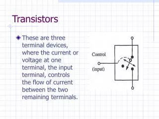
Transistors. These are three terminal devices, where the current or voltage at one terminal, the input terminal, controls the flow of current between the two remaining terminals. Transistors. Can be classified as: FET – Field Effect Transistor; Majority carrier device; Unipolar device;

Transistors
E N D
Presentation Transcript
Transistors • These are three terminal devices, where the current or voltage at one terminal, the input terminal, controls the flow of current between the two remaining terminals.
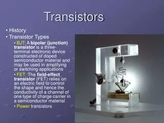
Transistors • Can be classified as: • FET – Field Effect Transistor; • Majority carrier device; • Unipolar device; • BJT – Bipolar Junction Transistor; • Minority carrier device; • Bipolar device.
FETs • Two primary types: • MOSFET, Metal-Oxide-Semiconductor FET. Also known as IGFET – Insulated Gate FET; • JFET, Junction FET. • MOS transistors can be: • n-Channel; • Enhancement mode; • Depletion mode; • p-Channel; • Enhancement mode; • Depletion mode;
MOSFET • MOSFETs are identified by symbols like the ones shown below:
MOSFET Operation • Voltage at gate controls the flow of current between drain and source. • VGS – Voltage between gate and source. • VDS – Voltage between drain and source.
MOSFET Operation • When VGS = 0 then no current flows between drain and source. • pn-Junction is reverse biased.
Threshold Voltage • The value of VGS where the drain current just begins to flow. • Typical values: • 0.3 to 0.8 volts.
MOSFET Operation • Two cases: • Ohmic region: • Active Region:
MOSFET Operation • Ohmic Region:
MOSFET Operation • Active Region:
K Parameter • The constant K, called the conductance parameter, is measured in units of mA/V2. • Where:
MOSFET Output Curves • A family of curves representing the V-I characteristics of transistors. • A plot of drain current, ID, as a function of drain-to-source voltage, VDS, for several values of VGS.
P-Channel Enhancement MOSFET • Note the n-type body and the p-type source and drain areas. • Both VGS and VDD are negative with respect to ground.
Depletion Mode MOSFETs • n-Channel is built in. • VGS varies from negative values to positive values, where negative values of VGS depletes the channel while positive values enhance it further.
JFETs • Depletion-mode FET with a different structure than that of the MOSFET. • Not generally used for switching elements of digital circuits. • Used in special applications such as analog circuits where very high input impedance is required.
JFETs • Every p-n junction has a depletion region devoid of carriers, and the width of the depletion region can be controlled by the applied voltage across the junction.
JFETs • Note the highest value of VGS. • What happens if you make VGS positive with respect to ground.
Inverter Circuit • This circuit is designated as the common source configuration. It is used in digital circuits.
Inverter Circuit • When Vinis low the transistor is off and Voutis high. • When Vinis high the transistor is on and Voutis low.
MOSFET Circuit Model For Switching • VGS controls the switch in the model and ron is defined as:
Inverter Circuit • For RL = 1KΩ, and VDD=5V.
Large Signal Amplifiers • DC biasing: • Ensuring that the transistor has the correct dc level at its terminals. • Termed as setting the Q-point, quiescent operating bias point. • Same as setting the dc voltages and currents for the circuit with no signal applied.
Large Signal Amplifiers • The dc bias voltages and currents must be maintained even when the circuit is confronted with: • Sources variations; • Temperature changes; • Change in component values due to manufacturing process inconsistencies.
Self-Bias Circuit • Useful for devices that require a negative gate-to-source voltage (depletion mode n-channel devices). • Negative gate-to-source voltages are achieved by raising the source voltage higher than the gate voltage.
Procedure • Draw load line on the output curves of the transistor. • Locate the Q-point on the load line. • If there is a bypass capacitor in the circuit, then construct an ac load line with slope: • Calculate the large signal voltage gain.
BJTs • Invented in 1947 in the Bell Laboratories. • It revolutionized electronics, by replacing the vacuum tubes. • Standard for the TTL (Transistor-Transistor-Logic) and ECL (Emitter-Coupled-Logic) families of logic devices.
BJT Structure • Three-layer sandwich of alternating semiconductor materials. • Two types: • NPN; • PNP. • Terminals: • Emitter; • Base; • Collector.
BJT Structure • Two p –n junction diodes built very close together. • The junction between base and emitter is called emitter junction, and the junction between base and collector is called collector junction.
BJT Structure • The emitter is placed on top of the collector with a very thin base between them, and the primary carrier flow is from the emitter to the collector.
Modes of Operation • Cutoff – Both junctions are reverse biased and the transistor appears as an open switch. • Saturation – Both junctions are forward biased and the transistor appears as a closed switch. • These two bias conditions are important for digital circuits.
BJT Working as a Switch • Note the simplified interpretation of the BJT working as a switch in cutoff and saturation.
BJT Models for Switching • IB(SAT)- the minimum base current to be exceeded for the transistor to be considered in saturation mode.
Modes of Operation • Active – The emitter junction is forward biased and the collector junction is reverse biased. • Reverse active – The emitter junction is reverse biased and the collector junction is forward biased.
Common Source Amplifier • Non-linear. • Large variations in beta. • Thermal runaway.
Self-Bias Circuit • Useful to control the effects discussed in the previous slide. • This circuit stabilizes collector current instead of base current, thus reducing the effects of beta variations and temperature on the quiescent operating point. • Collector current is determined by the voltage across a resistor, RE, placed in series with the emitter.
Procedure • Draw load line on the output curves of the transistor. • Locate the Q-point on the load line. • If there is a bypass capacitor in the circuit, then construct an ac load line with slope: • Calculate the large signal voltage gain.