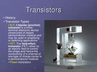
Transistors
Transistors. Camille Cruz Chase Thompson Tyler Nelson September 26, 2013. Outline. Introduction Transistors Types Bipolar Junction Transistors Field Effect Transistors Power Transistors Example. What is a Transistor?. Transistors. First Transistor. Different types and sizes.


Transistors
E N D
Presentation Transcript
Transistors Camille Cruz Chase Thompson Tyler Nelson September 26, 2013
Outline • Introduction • Transistors Types • Bipolar Junction Transistors • Field Effect Transistors • Power Transistors • Example
Transistors First Transistor Different types and sizes FET and BJT Transistor BJT (PNP) Electrical Diagram Modern Electronics
Purpose • To amplify and switch electronic signals on or off (high or low) • Modern Electronics Microprocessor Motor Controllers Cell Phones
Vacuum tubes • Purpose • Used as signal amplifiers and switches • Advantages • High power and frequency operation • Operation at higher voltages • Less vulnerable to electromagnetic pulses • Disadvantages • Very large and fragile • Energy inefficient • Expensive
Invention • Evolution of electronics • In need of a device that was small, robust, reliable, energy efficient and cheap to manufacture • 1947 • John Bardeen, Walter Brattain and William Schockly invented transistor • Transistor Effect • “when electrical contacts were applied to a crystal of germanium, the output power was larger than the input.”
Doping • Process of introducing impure elements (dopants) into semiconductor wafers to form regions of differing electrical conductivity Negatively charged Semiconductor Positively charged semiconductor
Doping Effects • P-type semiconductors • Created positive charges, where electrons have been removed, in lattice structure • N-type semiconductors • Added unbound electrons create negative charge in lattice structure • Resulting material • P-N junction
P-N junction Forward Biasing Reverse Biasing
P-N junction • Controls current flow via external voltage • Two P-N junctions (bipolar junction transistor, BJT) • Controls current flow and amplifies the current flow
Transistor Categories • Semiconductor material • Structure • Polarity • Maximum power rating • Maximum operating frequency • Application • Physical packaging • Amplification factor
Types of Transistors • Bipolar Junction Transistor (BJT) • Field Effect Transistors (FET) • Power Transistors
BJT Introduction • Bipolar Junction Transistors (BJT) consists of three “sandwiched” semiconductor layers • The three layers are connected to collector (C), emitter (E), and base (B) pins • Current supplied to the base controls the amount of current that flows through the collector and emitter
BJT Schematic NPN • NPN • BE forward bias • BC reverse bias • PNP • BE reverse bias • BC forward bias PNP
BJT Characteristic Curves Transfer Characteristic • Characteristic curves can be drawn to show other useful parameters of the transistor • The slope of ICE / IBEis called the Transfer Characteristic (β)
BJT Characteristic Curves Input Characteristic • The Input Characteristic is the base emitter current IBE against base emitter voltage VBE • IBE/VBEshows the input Conductance of the transistor. • The increase in slope of when the VBE is above 1 volt shows that the input conductance is rising • There is a large increase in current for a very small increase in VBE.
BJT Characteristic Curves Output Characteristic • collector current (IC) is nearly independent of the collector-emitter voltage (VCE), and instead depends on the base current (IB) IB4 IB3 IB2 IB1
BJT Applications BJT Switch • Offer lower cost and substantial reliability over conventional mechanical relays. • Transistor operates purely in a saturated or cutoff state (on/off) • This can prove very useful for digital applications (small current controls a larger current)
BJT Applications BJT Amplifier
BJT Applications BJT Amplifier
Field Effect Transistors (FET) Chase Thompson
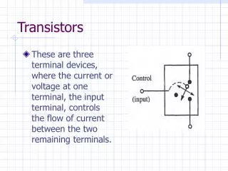
FET Basics • Electric Field • Voltage Controlled • FET includes three distinct pieces • Drain • Source • Gate
FET versus BJT? • Difference: • Voltage vs Current Input • Unipolar vs Bipolar • Noise • Higher input impedance • Fragile and low gain bandwidth Same: • Applications: amplifier, switch, etc. • Relies on PNP or NPN junctions to allow current flow
JFET • Reverse Biased PN-junction • Depletion mode devices • Creates a potential gradient to restrict current flow. (Increases overall resistance) http://www-g.eng.cam.ac.uk/mmg/teaching/linearcircuits/jfet.html
JFET • N-channel JFET • P-channel JFET uses same principles but • Channel current is positive due to holes instead of electron donors • Polarity of biasing voltage must be reversed
JFETs Characteristics and Applications of FETs • Simplest type of FET – easy to make • High input impedance and resistance • Low Capacitance • Slower speed in switching • Uses? • Displacement sensor • High input impedance amplifier • Low-noise amplifier • Analog switch • Voltage controlled resistor
MOSFET p-channel • Similar to JFET • A single channel of single doped SC material with terminals at end • Gate surrounds channel with doping that is opposite of the channel, making the PNP or NPN type • BUT, the MOSFET uses an insulator to separate gate from body, while JFET uses a reverse-bias p-n junction n-channel MOSFETenhanced mode MOSFETdepleted mode
How does a MOSFET work? No Voltage to Gate Voltage to Gate Source Drain Source Drain n n Simplified Notation No current flow “Short” allows current flow
MOSFET Triode Mode/Linear Region VGS > Vth and VDS < ( VGS - Vth ) Saturation/Active Mode VGS > Vth and VDS > ( VGS - Vth ) VGS : Voltage at the gate Vth : Threshold voltage VDS : Voltage from drain to source μn: charge-carrier effective mobility W: gate width L: gate length Cox : gate oxide capacitance per unit area λ : channel-length modulation parameter
MOSFETs Characteristics and Applications of FETs • Oxide layer prevents DC current from flowing through gate • Reduces power consumption • High input impedance • Rapid switching • More noise than JFET • Uses? • Again, switches and amplifiers in general • The MOSFET is used in digital CMOS logic, which uses p- and n-channel MOSFETs as building blocks • To aid in negating effects that cause discharge of batteries Use of MOSFET in battery protection circuit
Power Transistors • Concerned with delivering high power • Used in high voltage and high current application • In general • Fabrication process different in order to: • Dissipate more heat • Avoid breakdown • Different types: Power BJTs, power MOSFETS, etc.
References (32) http://www.utdallas.edu/research/cleanroom/TystarFurnace.htm http://www.osha.gov/SLTC/semiconductors/definitions.html http://www.products.cvdequipment.com/applications/diffusion/1/ http://amath.colorado.edu/index.php?page=an-immersed-interface-method-for-modeling-semiconductor-devices http://www.extremetech.com/article2/0,2845,1938467,00.asp http://macao.communications.museum/eng/Exhibition/secondfloor/moreinfo/2_10_3_HowTransistorWorks.html http://fourier.eng.hmc.edu/e84/lectures/ch4/node3.html http://www.appliedmaterials.com/htmat/animated.html http://hyperphysics.phy-astr.gsu.edu/hbase/solids/dope.html#c3 http://www.tpub.com/neets/book7/25.htm http://esminfo.prenhall.com/engineering/wakerlyinfo/samples/BJT.pdf http://web.engr.oregonstate.edu/~traylor/ece112/lectures/bjt_reg_of_op.pdf http://www.me.gatech.edu/mechatronics_course/transistors_F09.ppt http://en.wikipedia.org/wiki/Bipolar_junction_transistor http://en.wikipedia.org/wiki/Common_emitter http://en.wikipedia.org/wiki/Diode http://www.kpsec.freeuk.com/trancirc.htm http://en.wikipedia.org/wiki/Field-effect_transistor http://en.wikipedia.org/wiki/JFET http://en.wikipedia.org/wiki/MOSFET http://www.slideshare.net/guest3b5d8a/fets http://www.rhopointcomponents.com/images/jfetapps.pdf http://cnx.org/content/m1030/latest/ http://www.play-hookey.com/semiconductors/enhancement_mode_mosfet.html http://www.youtube.com/watch?v=-aHnmHwa_6I&feature=related http://www.youtube.com/watch?v=v7J_snw0Eng&feature=related http://info.tuwien.ac.at/theochem/si-srtio3_interface/si-srtio3.html http://hyperphysics.phy-astr.gsu.edu/hbase/solids/dope.html#c4 http://inventors.about.com/library/inventors/blsolar5.htm http://thalia.spec.gmu.edu/~pparis/classes/notes_101/node100.html http://hyperphysics.phy-astr.gsu.edu/hbase/solids/pnjun.html#c3 http://science.jrank.org/pages/6925/Transistor.html