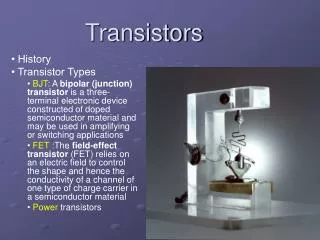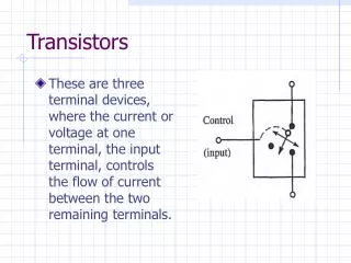
Transistors
ME 4447/6405 Student Lecture. Justin Chow Jacob Huang Daniel Soledad. Transistors . Overview. History Properties Types BJT JFET MOSFET Applications. Daniel Soledad. Introduction. Transistor History “Transistor” is combination of “transconductance” and “variable resistor”

Transistors
E N D
Presentation Transcript
ME 4447/6405 Student Lecture Justin Chow Jacob Huang Daniel Soledad Transistors
Overview • History • Properties • Types • BJT • JFET • MOSFET • Applications Daniel Soledad
Introduction • Transistor History • “Transistor” is combination of “transconductance” and “variable resistor” • How Transistors Are Made • Vacuum tubes • Inefficient, fragile, bulky, generated a lot of heat • First Transistors • Semiconductors – Bell Labs 1947
Introduction • Packaging • Surface Mount or Through Hole • Usually 3 or 4 terminal device • Can be packaged into ICs • General Applications • Amplification /Regulation • Switches
General Operation • Current Controlled • i.e: BJT • The output current is proportional to input current • Voltage Controlled • i.e.: JFET, MOSFET • The output current is proportional to input voltage
BJT Transistor Justin Chow • Bipolar Junction Transistor • 3 semiconductor layers sandwiched together • Comes in two flavors NPN BJT PNP BJT
BJT Transistor • Diodes Forward Biased Reverse Biased current flows no current flows when VPN > .6-.7V
emitter base collector Electron Flow BJT Transistor • BJT Basics (NPN) • BE Forward Biased • BC Reversed Biased • β=IB / Ic ≈ 100 • IE = IB + IC
BJT Transistor • Things to remember • PNP, biasing opposite • Conventional current vs electron flow • A small input current controls a much larger output current.
BJT Transistor Operating Regions
BJT Transistor Operating Regions
Application: Switching • From 3rd Exercise • Turns on/off coils digitally
BJT Transistor β=100 Common Emitter Amplifier
BJT Transistor • IB = (Vin − VB) / 10000Ω = (Vin − 0.7) / 10000Ω • IC = β(Vin − 0.7) / 10000Ω • Vout=10000*(Vin-0.7)/1000 • When VCE = 0.2V • IC = 9.8 / 1000Ω = 9.8mA • IB = IC / β = 0.098mA • Vin − 0.7 = (0.098mA)(10000Ω) • Vin = 1.68V or greater. Common Emitter Amplifier
BJT Transistor • Power Dissipation • PBJT = VCE * iCE • Should be below the rated transistor power • Important for heat dissipation as well
Darlington Transistors Increased Gain β = β1 * β2 VBE = VBE1 + VBE2 Slower Switching 2N6282
FET Transistors Analogous to BJT Transistors Output is controlled by input voltage rather than by current 4 Pins vs. 3
FET Transistors FET (Field Effect Transistors) MOSFET (Metal-Oxide-Semiconductor Field-Effect Transistor) JFET (Junction Field-Effect Transistor) MESFET HEMT MODFET Most common are the n-channel MOSFET or JFET Jacob Huang
FET Transistors – Circuit Symbols In practice the body and source leads are almost always connected Most packages have these leads already connected D D D B G G B G S S S MOSFET JFET
MOSFET Metal-Oxide Semiconductor F.E.T. A.K.A. Insulated-Gate FET (IGFET) 2 Modes: Enhancement/Depletion
Depletion Mode • N-Channel • + Vgs -> More electrons -> More Current • - Vgs -> Less electrons -> Less current • P-Channel – Reversed • Different from BJT
Characteristic Curves for D-type D G B S Current flow
Enhancement Mode • N-Channel • VGS > Vth -> Turns on device • VGS < VTH -> No Current • P-Channel • Reversed • Only E-type used now
Modes of Operation D G B S Current flow
Characteristic Curve for E-type D G B S Current flow
Power MOSFET • Used in high-power applications • Heat Sink • Vertical layout • Not Planar like other transistors
Junction gate FET Reverse Bias VGS => Reduces channel size => Reduced Current Defaults “on”
JFET as Switch Vgs = 0 “on” |Vgs|> |Vp| “off” Vp = Pinch-off or Cut-off Voltage
JFET Properties • Internal Capacitance • Bi-directional • Cut-off voltage is varying for each JFET • 0.3V – 10V • N-Channel – Negative VGS • P-Channel – Positive VGS • Do not Forward Bias JFET – burn out
CMOS Complementary MOS Used in Logic Gates P-channel (PMOS) to high N-channel (NMOS) to low HIGH usually +5 V LOW usually ground Q is high when A = 0, Q is low when A = 1
References Spring 2007/2008 Slides http://www.made-in-china.com/image/2f0j00ZhaTKREnIQkfM/IC-Transistor.jpg http://en.wikipedia.org/wiki/JFET http://en.wikipedia.org/wiki/MOSFET http://en.wikipedia.org/wiki/Bipolar_junction_transistor http://www.allaboutcircuits.com/vol_3/chpt_2/8.html http://www.mcmanis.com/chuck/robotics/tutorial/h-bridge/images/basic-bjt.gif&imgrefurl=http://www.mcmanis.com/chuck/robotics/tutorial/h-bridge/bjt_theory.html http://www.allaboutcircuits.com/vol_3/chpt_2/6.html http://web.engr.oregonstate.edu/~traylor/ece112/lectures/bjt_reg_of_op.pdf http://hades.mech.northwestern.edu/wiki/index.php/Diodes_and_Transistors#Common_Emitter_Amplifier_Circuit http://en.wikipedia.org/wiki/Darlington_transistor http://www.allaboutcircuits.com/vol_3/chpt_6/2.html http://www.allaboutcircuits.com/vol_3/chpt_4/2.html http://www.designers-guide.org/Forum/YaBB.pl?num=1162476437/4 http://en.wikipedia.org/wiki/CMOS