SNAP Data Recorder
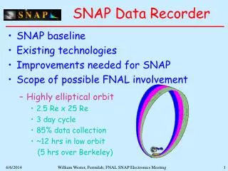
SNAP Data Recorder. SNAP baseline Existing technologies Improvements needed for SNAP Scope of possible FNAL involvement Highly elliptical orbit 2.5 Re x 25 Re 3 day cycle 85% data collection ~12 hrs in low orbit (5 hrs over Berkeley). SNAP Baseline.

SNAP Data Recorder
E N D
Presentation Transcript
SNAP Data Recorder • SNAP baseline • Existing technologies • Improvements needed for SNAP • Scope of possible FNAL involvement • Highly elliptical orbit • 2.5 Re x 25 Re • 3 day cycle • 85% data collection • ~12 hrs in low orbit (5 hrs over Berkeley) William Wester, Fermilab, FNAL SNAP Electronics Meeting
SNAP Baseline • “A solid state recorder – a shoebox” • No moving (rotating) parts • Lots of memory • Radiation / space qualified • Low power • SNAP plans to transmit data in Ka band @ 150-300 Mbs with 6W transmitter. • 375 Gbyte (Levi, DOE talk) might grow to ~500 Gbyte storage (expanded science). William Wester, Fermilab, FNAL SNAP Electronics Meeting
Memory technologies • Memories • Dynamic RAM • Parasitic capacitance needs power to refresh • Static RAM • 2 transistors + 4 resistors FLIP-FLOP • FLASH memories • Floating gate with tunneling processes • FeRAM • Ferromagnetic crystal storage • Holographic and other technologies • Tape and disk recorders are candidates William Wester, Fermilab, FNAL SNAP Electronics Meeting
Some current missions • Cassini • Two SSRs each of 2.5 Gbit • 640 4Mbit DRAMs • Early 90’s technology => ’97 launch • Multiple-bit upsets observed despite testing (architecture flaw) • 3 control ASICs • 120 DRAM/board • Error detection and • correction circuitry William Wester, Fermilab, FNAL SNAP Electronics Meeting
Some current missions • Hubble Space Telescope • Reel-to-reel tape replaced by SSR • 1.2 Gb -> 12 Gb • 1440 16 Mbit DRAM • Two stacks of 10 (+2 spare) for 320 Mb packages (still 12500 chips for 500 GB) • Single event upsets observed • EDAC (Reed-Solomon scheme) • Two events where memory corrected but damaged • Kepler (earth size planets transiting stars) • Large CCD array, but only star’s pixels Xmit’d William Wester, Fermilab, FNAL SNAP Electronics Meeting
Challenges for SNAP • Amount of memory • No examples of large (>>1 GB) SSRs found • Moore’s Law growth. Need ~4000 x 1 Gbit • Mass budget • Boards with 1000’s of chips is several 10’s lbs • Power budget • Need more information • Radiation tolerance • Space qualification William Wester, Fermilab, FNAL SNAP Electronics Meeting
Radiation Tolerance • Ionizing radiation small (<50 Krad) • SEE (Single Event Effects) include many failure mechanisms • SEU (Single Event Upset) can change state of a bit SRAM Sensitive area DRAM Sensitive area William Wester, Fermilab, FNAL SNAP Electronics Meeting
Radiation Tolerance • FLASH memories • Very thin oxides make FLASH susceptible • Charge pump is the suspect for many failures • Limited number of read/write cycles William Wester, Fermilab, FNAL SNAP Electronics Meeting
Space qualification • Thermal-Vac • Vacuum and Temperature extremes (-40 to +90 degC) • Vibration facility • Hard shake • More Thermal-Vac and vibration testing after mount • Room filled with engine noise simulation HST HOST Mission William Wester, Fermilab, FNAL SNAP Electronics Meeting
Space qualification William Wester, Fermilab, FNAL SNAP Electronics Meeting
Space qualification William Wester, Fermilab, FNAL SNAP Electronics Meeting
Space qualification William Wester, Fermilab, FNAL SNAP Electronics Meeting
FNAL Involvement • Large robust memory is nicely associated with expanded science program of deep field sky survey • Radiation issues (tie-in with shield) are already studied at FNAL • Next steps • Continue to get working knowledge • Contact vendors • Narrow technologies to working concept • ASIC resources are possible William Wester, Fermilab, FNAL SNAP Electronics Meeting
Conclusions • No clear technology solution • High density, low power, radiation hard • Flash memories x10 less power (big difference between 100 W and 1 kW) • New concepts not ready for 1 Gb scale • Dense technologies use smaller feature sizes that are more prone to some failures • ASIC solution is possible, but could memories be made dense enough with accessible minimal feature sizes William Wester, Fermilab, FNAL SNAP Electronics Meeting