The Future of Organic Electronics
190 likes | 1.55k Vues
The Future of Organic Electronics. Jaya Movva Ben Spearin Jon Anderson Joshua Wrazen . Inorganic vs. Organic. Organic electronics, or plastic electronics, is the branch of electronics that deals with conductive polymers, which are carbon based.

The Future of Organic Electronics
E N D
Presentation Transcript
The Future of Organic Electronics Jaya Movva Ben Spearin Jon Anderson Joshua Wrazen
Inorganic vs. Organic • Organic electronics, or plastic electronics, is the branch of electronics that deals with conductive polymers, which are carbon based. • Inorganic electronics, on the other hand, relies on inorganic conductors like copper or silicon. Silicon sample Carbon sample
Benefits and Obstacles • Organic electronics are lighter, more flexible, and less expensive than their inorganic counterparts. • They are also biodegradable (being made from carbon). • This opens the door to many exciting and advanced new applications that would be impossible using copper or silicon. • However, conductive polymers have high resistance and therefore are not good conductors of electricity. • In many cases they also have shorter lifetimes and are much more dependant on stable environment conditions than inorganic electronics would be.
Organic Electronic $5 / ft2 Low Capital 10 ft x Roll to Roll Flexible Plastic Substrate Ambient Processing Continuous Direct Printing Silicon $100 / ft2 $1-$10 billion < 1m2 Rigid Glass or Metal Ultra Cleanroom Multi-step Photolithography Cost Fabrication Cost Device Size Material Required Conditions Process http://www.xeroxtechnology.com/ip1.nsf/sedan1?readform&unid=2D1FF1AC91C40AA985256D1A00616714
Organic Light Emitting Diodes (OLEDs) • An OLED is a thin film LED in which the emissive layer is an organic compound. • When this layer is polymeric (or plastic), OLEDs can be deposited in rows and columns on a screen using simple printing methods that are much more efficient than those used in manufacturing traditional LEDs. • A key benefit of OLEDs is that they don’t need a backlight to function.
How it Works • An electron and hole pair is generated inside the emissive layer by a cathode and a transparent anode, respectively. • When the electron and hole combine, a photon is produced, which will show up as a dot of light on the screen. • Many OLEDs together on a screen make up a picture
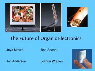
Less expensive to produce • Wide range of colors and viewing angle • Consumes much less energy than traditional LCDs. • Flexible and extremely thin • Limited lifetime of about 1,000 hours. • Susceptible to water
Organic transistors • INTRODUCTION Organic transistors are transistors that use organic molecules rather than silicon for their active material. This active material can be composed of a wide variety of molecules. • Advantages of organic transistors: • Compatibility with plastic substances • Lower temperature is used while manufacturing (60-120°C) • Lower cost and deposition processes such as spin-coating, printing and evaporation • Less need to worry about dangling bonds( simplifies the process) • Disadvantages of organic transistors: • Lower mobility and switching speeds compared to Si wafers • Usually does not operate under invasion mode. Example of an organic transistor (on the side)
Organic Thin film transistors(OTFTS) • TFTs are transistors created using thin films, usually of silicon deposited on glass. The deposited silicon must be crystallized using laser pulses at high temperatures. OTFTs active layers can be theramlly evaporated and deposited on any organic substrate (a flexible piece of plastic) at much lower temperatures. • Benefits of an OTFT: • Does not require glass substrate as amorphous Si does. It could be made on a piece of plastic. • Manufactured at lower temperatures • Deposition techniques could reduce costs dramatically. • Challenges involved: • Workarounds for complications with photo resists. • To find organic semiconductors with high enough mobilities and switching times.
Pictureof an OTFT made on a plastic substrate • FUTURE • OTFT technology’s application is diverse. Organic thin-film transistor (OTFT) technology involves the use of organic semiconducting compounds in electronic components, notably computer displays. Such displays are bright, the colors are vivid, they provide fast response times (which need to be developed in OTFT), and they are easy to read in most ambient lighting environments. • Organic substrates allow for displays to be fabricated on flexible surfaces, rather than on rigid materials as is necessary in traditional TFT displays. A piece of flexible plastic might be coated with OTFT material and made into a display that can be handled like a paper document. Sets of such displays might be bundled, producing magazines or newspapers whose page contents can be varied periodically, or even animated. This has far-reaching ramifications. For example, comic book characters might move around the pages and speak audible words. More likely, such displays will find use in portable computers and communications systems.
Production and Applications • Quicker Checkout • Inventory Control • Reduced Waste • Efficient flow of goods from manufacturer to consumer
Production Specifications of Manufacturing a Nano-RFID • > 96 bits • Four main communication Bands: 135KHz, 13.56MHz, 900MHz, 2.4 GHz • Vacuum Sublimation
The Future of Organic Electronics http://www.orgatronics.com/organic_electronics.html
The Future of Organic Electronics Smart Textiles Integrates electronic devices into textiles, like clothing Made possible because of low fabrication temperatures Has many potential uses, including: Monitoring heart-rate and other vital signs, controlling embedded devices (mp3 players), keep the time… http://www.orgatronics.com/smart_fabrics.html
The Future of Organic Electronics Lab on a Chip A device that incorporates multiple laboratory functions in a single chip Organic is replacing some Si fabrication methods: -Lower cost -Easier to manufacture -More flexible http://www.orgatronics.com/lab_on_chip.html
The Future of Organic Electronics Portable, Compact Screens Screens that can roll up into small devices Black and White prototype already made by Philips(the Readius™ at the bottom-left) Color devices will be here eventually http://jscms.jrn.columbia.edu/cns/2005-04-05/gencer-plasticelectronics http://www.polymervision.com/Technology/downloads/Index.html
References • http://whatis.techtarget.com/definition/0,,sid9_gci512140,00.html • students.washington.edu/jetpeach/ EE341_Organic_Transistors_Presentation.ppt • http://www.chem.uky.edu/research/anthony/tft.html • http://en.wikipedia.org/wiki/OLED • www.tagsysrfid.com
