Analytical and Simulation Analysis of PN-Junction Diode Characteristics
This document presents a detailed analysis of a pn-junction diode with uniform doping concentrations (NA=ND=10^16 cm^-3) and a region length of 1 µm. The study involves calculating and simulating the built-in voltage (Vbi), total depletion region width (W), and maximum electric field at the junction. Results are compared between analytical calculations and simulation outcomes for different scenarios, including equilibrium conditions, bias effects, and non-symmetric junctions. This comprehensive examination provides valuable insights into diode behavior under various conditions.

Analytical and Simulation Analysis of PN-Junction Diode Characteristics
E N D
Presentation Transcript
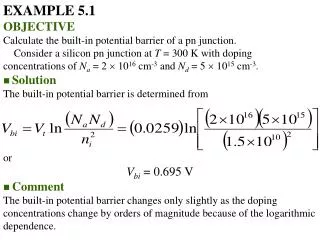
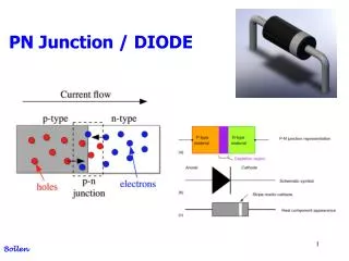
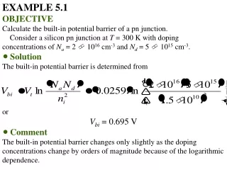
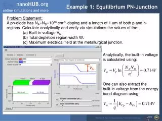
Example 1: Equilibrium PN-Junction Problem Statement: A pn-diode has NA=ND=1016 cm-3 doping and a length of 1 um of both p and n-regions. Calculate analytically and verify via simulations the values of the: (a) Built-in voltage Vbi (b) Total depletion region width W. (c) Maximum electrical field at the metallurgical junction. Analytically, the built-in voltage is calculated using: Vbi One can also extract the built-in voltage from the energy band diagram using:
Example 1: Charge Density W Question1: What is the analytical value of the total depletion region width? Answer1: The analytical value of the depletion region width is 0.432 um. Question2: What is the extracted simulated value of the total depletion region width? Answer2: The simulated value of the depletion region width is ~ 0.43 um.
Example 1: Electric Field Profile Emax Question1: What is the analytical value of the peak electric field? Answer1: The analytical value of the peak electric field is 33.14 kV/cm. Question2: What is the extracted simulated value of the peak electric field? Answer2: The simulated value of the peak electric field is 32 kV/cm.
Example 2: PN-Junction Under Bias Problem Statement: A pn-diode has NA=ND=1016 cm-3 doping and a length of 1 um of both p and n-regions. Simulate: (a) Energy band profile under applied bias VA=0.6 V (b) quasi-Fermi level variation with position (c) electric field under bias (d) forward IV-characteristic of the diode The net built-in voltage is: Vbi - VA = 0.714 -0.6 = 0.114 V The value extracted from the graph for the net built-in voltage is 0.115 V.
Example 2: Quasi-Fermi Level Variation Question: Where is the variation of the quasi-Fermi levels significant? Answer: The variation of the quasi-Fermi levels is significant in regions in which the carrier concentration changes by orders of magnitude.
Example 2: Electric Field Under Bias Question1: Compare the equilibrium and non-equilibrium values of the field! Answer1: The peak non-equilibrium field is lower. Question2: Compare the equilibrium and nonequilibrium depletion region widths! Answer2: The non-equilibrium depletion region with is smaller under forward bias.
Example 2: Current Density Question: How does the current vary with increasing the doping density of either the p- or n-region, or both? Answer: With increasing the doping density of either the p-side, or the n-side, or both, the potential barrier for the minority carriers increases and the current decreases.
Example 3: Non-Symmetric Junction Problem Statement: A pn-diode has NA=1016 cm-3 and ND=1018 cm-3 doping, and a length of 1 um of both p and n-regions. Simulate: (a) equilibrium energy band profile (b) charge density, to see the extent of the depletion regions (c) electric field profile to examine the contribution of the inversion charge
W Example 3: Charge Density Question1: What is the analytical value of the total depletion region width? Answer1: The analytical value of the depletion region width is0.327 um. Question2: What is the extracted simulated value of the total depletion region width? Answer2: The extracted simulated value of the depletion region width is ~ 0.31 um.
Example 3: Electric Field Profile Inversion charge Depletion charge Question1: What is the analytical value of the peak electric field? Answer1: The analytical value of the peak electric field is 50.2 kV/cm. Question2: What is the extracted simulated value of the peak electric field? Answer2: The simulated value of the peak electric field is 67.1 kV/cm.
Example 4: Series Resistance Problem statement: In this exercise we will examine the series resistance effects under high bias conditions. The p-side doping is NA=1016 cm-3 and the n-side doping is ND=1016 cm-3. The length of the p-side and the n-side region is taken to be 1 um. Plot the following variables: (a) Conduction band, valence band and the intrinsic level variation vs. position for applied bias VANODE=1.2 V. (b) Quasi-Fermi level variation. (c) Forward IV-characteristics of a diode for applied bias between 0 and 1.2 V in 0.05 V increments. From the forward IV-characteris- tics under high bias conditions extract the series resistance.
Example 4: Current Density Series resistance effect Ideal characteristics
V1 V2 Example 4: Current Density, Cont’d The ideal diode current is The non-ideal diode current is: V=V2-V1=RID => R= V/ID From the equality of the currents we have: