PN Junction / DIODE
PN Junction / DIODE. Bollen. SEMICONDUCTOR Pure silicium P material boron doped N material stibium doped P material and N material PN junction PN junction layer 0V7 PN junction characteristic. DIODE characteristic DIODE DC and ac resistance DIODE load line DIODE flipped resistorline

PN Junction / DIODE
E N D
Presentation Transcript
PN Junction / DIODE Bollen
SEMICONDUCTOR Pure silicium P material boron doped N material stibium doped P material and N material PN junction PN junction layer 0V7 PN junction characteristic DIODE characteristic DIODE DC and ac resistance DIODE load line DIODE flipped resistorline DIODE DC resistance DIODE ac resistance AGENDA Bollen
Pure silicium • 4 electrons • Ideal is to have 8 • So share withyourneighbour • Co-valencebounding • Electricalneutral Semiconductor, pure silicium Bollen
Pure silicium • 4 electrons • Ideal is to have 8 • So share withyourneighbour • Co-valencebounding • Electricalneutral Semiconductor, pure silicium Bollen
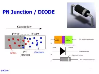
P material = silicium (+4) boron (+3) doped Boron misses 1 positvie charge (positon) & 1 negative charge (electron) Co-valence bounding Electrical neutral P material misses one electron, or has a place for one electron, this is called a free hole Semiconductor, P material boron doped Bollen
N material = silicium (+4) stibium (+5) doped Stibium has got extra 1 positive charge (positon) & 1 negative charge (electron) Co-valence bounding Electrical neutral N material has got one extra electron out of the bounding, this is called a free electron Semiconductor, N material stibium doped Bollen
P material = Free holes N material = Free electrons P material and N material Bollen
PN junction Anode = P=material Kathode = N material KNAP = handsome K = Negative A = Positive Bollen
Depletion layer can be made Wider by external reverse voltage Smaller by External froward voltage Depletion layer; Uth = 0V7 PN junction, depletion layer 0V7 Bollen
Forward Depletion layer is gone Ud > 0V7 Current can flow Reverse Depletion layer is wider Ud < 0V0 Current can NOT flow PN junction, characteristic Bollen
a Diode Is a one way street for current Diode, characteristic Bollen
Assumption Treshold Voltage for silicium Ud = 0V7 for germanium Ud = 0V2 Diode, characteristic Bollen
Diode, characteristic Where id = diode current Vd= diode voltage KT/q = 26 mV Iss = leakage current (1uA) Bollen
Diode, DC and ac resistance Bollen
Diode, Load line How to calculate the exact value of vd and id; Graphical; use load line, indicates the load of the diode Bollen
Diode, Load line For shure id = ir = i For shure vs = vd + vr Bollen
For shure For shure id = ir = i vs = vd + vr Diode, Load line Bollen
Flip the resistor line and push the two curves horizontally to fit; vs = vd + vr Diode, Flipped resistor line Bollen
Diode, Load line The flipped resistor line is called LOAD-LINE Bollen
For DC resistance use the load line method For large voltages normally Vd= 0V7 is used Diode, DC resistance Bollen
Diode, ac resistance Differentiating gives Rd = Δvd/Δid = 26 mV / Id Where kT/q = 26 mV Bollen