Download
1 / 35
400 likes | 887 Vues
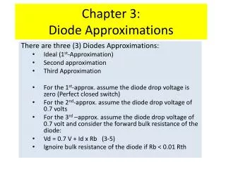
EKT 102 CHAPTER 3 SPECIAL-PURPOSE DIODE. 3. SPECIAL-PURPOSE DIODE. K. Cathode (K). +. V Z. I Z. −. Anode (A). A. 3.1 Zener Diode. Fig.3-1 : Zener diode symbol. Zener diode is a p-n junction diode that is designed to operate in the reverse breakdown region.

E N D
EKT 102 CHAPTER 3 SPECIAL-PURPOSE DIODE
3. SPECIAL-PURPOSE DIODE K Cathode (K) + VZ IZ − Anode (A) A 3.1 Zener Diode Fig.3-1: Zener diode symbol. • Zener diode is a p-n junction diode that is designed to operate in thereverse breakdown region. • Two things happen when the reverse breakdown voltage (VBR) is reached: • The diode current increases • drastically. • The reverse voltage (VR) across • the diode remains relatively • constant. • In other words, the voltage across a zener diode operated in this region is relatively constant over a range of reverse current and nearly equal to its zener voltage (VZ) rating. VBR Fig.3-2: Zener diode voltage-curent (V-I) characteristic.
3. SPECIAL-PURPOSE DIODE • 3.1.1 Zener Breakdown • There are two types of reverse breakdown: • Avalanche breakdown. • Zener breakdown. • Avalanche breakdown is a high-field effect that occurs when the electrostatic field • strength associated with the p-n junction is strong enough to pull electrons out of the • valence band within the depletion region. • Zener breakdown is a type of reverse breakdown that occurs at relatively low reverse • voltages. The n-type and p-type materials of a zener diode are heavily doped, resulting • in a very narrow depletion region. Therefore, the electric field existing within this region • is intense enough to pull electrons from their valence bands and create current at a low • reverse voltage (VR). • Note: • Zener diodes with low VZ ratings experience zener breakdown, while those with high VZ • ratings usually experience avalanche breakdown.
3. SPECIAL-PURPOSE DIODE IZ VZ VBR VR IZK Zener knee current IZT ΔIR Zener test current ΔVR IZM maximum Zener current 3.1.2 Breakdown Characteristics The characteristic that indicates the ability of the zener diode to keep the reverse voltage across its terminals nearly constant makes the diode is useful as a voltage regulator. Four main characteristics of the zener diode are: Zener voltage(VZ) is the nominal zener voltage at the breakdown voltage. Zener knee current (IZK) is the minimum current required to maintain the diode in breakdown for the voltage regulation. Zener test current (IZT) is the current level at which the VZ rating of the diode is measured. Zener maximumcurrent (IZM) is the maximum reverse current, which may not be exceeded. At this current level, the diode can work without being damaged or destroyed. Fig.3-3: Reverse characteristic of a zener diode.
3. SPECIAL-PURPOSE DIODE IF Fig.3-4: Ideal model and characteristic curve of a zener diode in reverse breakdown. VZ VR Fig.3-5: Practical model and characteristic curve of a zener diode, where the zener impedance (resistance), ZZ is included. VF The constant voltage drop = the nominal zener voltage. IR 3.1.3 Ideal-and-Practical Zener Equivalent Circuits A change in zener current (ΔIZ) produces a small changes in zener voltage (ΔVZ).
3. SPECIAL-PURPOSE DIODE 3.1.4 Temperature Coefficient The zener voltage of a zener diode is very sensitive to the temperature of operation. The formula for calculating the change in zener voltage due to a change in temperature is (3-1) where, VZ = nominal zener voltage at the reference temperature of 25oC. TC = temperature coefficient. T1 = new temperature level. T0 = reference temperature of 25oC. 3.1.4 Zener Power Dissipation and Derating The maximum current that may be carried by a given zener diode depends on both the zener voltage and the maximum dc power dissipation capability of the diode. The dc power dissipation of the zener diode is given by the formula, (3-2)
3. SPECIAL-PURPOSE DIODE The maximum power dissipation of a zener diode is specified for temperature at or below a certain value (50oC, for example). Above the specified temperature, the maximum power dissipation is reduced according to a derating factor. The derating factor is expressed in mW/oC. The maximum derated power can be determined with the following formula: (3-3)
3. SPECIAL-PURPOSE DIODE VOUT 3.2 Zener Diode Applications The zener diode can be used as a type of voltage regulator for providing stable reference voltages. 3.2.1 Zener Regulation with a Varying Input voltage Fig.3-6: Zener regulation with a no-load.
3. SPECIAL-PURPOSE DIODE For an ideal model of a certain zener diode, the minimum zener current (IZK) is specified on datasheet. However, the maximum zener current is not given on datasheet but can calculated from the maximum diode power specification, which is given on datasheet by using the equation: (3-4) For the minimum zener current, the voltage across the resistor is determined by: (3-5) Thus, the minimum input voltage that can be regulated by the zener diode, (3-6)
3. SPECIAL-PURPOSE DIODE For the maximum zener current, the voltage across the resistor is determined by: (3-7) Thus, the maximum input voltage that can be regulated by the zener diode, (3-8)
3. SPECIAL-PURPOSE DIODE 3.2.2 Zener Regulation with a Variable Load The zener diode maintains a nearly constant voltage across RL as long as the zener current is greater than IZK and less than IZM. Fig.3-7: Zener voltage regulation with a variable load When the output terminals of the zener regulator are open (RL = ∞) or a no-load condition, the load current (IL) = 0 and all of the current is through the zener. When a load resistor (RL) is connected, a part of the total current is through the zener and an other part through RL. As RL is decreased, the load current IL increases and IZ decreases. The zener diode continues to regulate the voltage until IZ reaches its minimum value, IZK. At this point IL is maximum, and a full-load condition exists.
3. SPECIAL-PURPOSE DIODE By using mathematically formula, when IZ is maximum, we obtain: (3-9) thus, (3-10) When IZ is minimum (IZ = IZK), so (3-11) (3-12)
3. SPECIAL-PURPOSE DIODE Fig.3-8. 3.2.3 Zener Regulation with a Variable Load In addition to voltage regulation applications, zener diode can be used in ac applications to limit voltage swings to desired levels. Part (a) shows a zener used to limit the positive peak of a signal voltage to the selected zener voltage. During the negative alternation, the zener acts as a forward-biased diode and limits the negative voltage to -0.7 V. When the zener is turned around, as in part (b), the negative peak is limited by zener action and the positive voltage is limited to +0.7 V. Two back-to-back zeners limit both peaks to the zener voltage ±0.7 V, as shown in part (c). During the positive alternation, D2 is functioning as the zener limiter and D1 is functioning as a forward-biased diode. During the negative alternation, the roles are reversed.
3. SPECIAL-PURPOSE DIODE 3.3 Varactor Diode Varactor is a type of p-n junction diode that operates in reverse bias. The capacitance of the junction is controlled by the amount of reverse bias. Varactor diodes are also referred to as varicapsor tuning diodesand they are commonly used in communication systems. 3.3.1 Basic Operation The capacitance of a reverse-biased varactor junction is found as: Fig.3-9: Varactor diode symbol (3-13) where, C = the total junction capacitance. A = the plate area. ε = the dielectric constant (permittivity). d = the width of the depletion region (plate separation). Fig.3-10: Reverse-biased varactor diode acts as a variable capacitor.
3. SPECIAL-PURPOSE DIODE The ability of a varactor to act as a voltage-controlled capacitor is demonstrated in Fig. 3-10. Fig.3-10: Varactor diode capacitance varies with reverse voltage. As the reverse-bias voltage increases, the depletion region widens, increasing the plate separation, thus decreasing the capacitance. When the reverse-bias voltage decreases, the depletion region narrows, thus increasing the capacitance.
3. SPECIAL-PURPOSE DIODE 3.3.2 Varactor Application A major application of varactor is in turning circuits, for example, VHF, UHF, and satelite receivers utilize varactors. Varactors are also used in cellular communications. When used in a parallel resonant circuit, as shown in Fig. 3-11, the varactor acts as a variable capacitor, thus allowing the resonant frequency to be adjusted by a variable voltage level. Fig.3-11: A resonant band-pass filter.
3. SPECIAL-PURPOSE DIODE • C1 prevents a dc path from potentiometer wiper back to the ac source through the • inductor and R1. • C2 prevents a dc path from cathode to the anode of the varactor through the inductor. • C3 prevents a dc path from the wiper to a load on the output through the inductor. • C4 prevents a dc path from the wiper to ground. • R2, R3, R4 and R5 function as a variable dc voltage divider for biasing the varactor. The parallel resonant frequency of the LC circuit is (3-14) where, L = the inductance of an inductor (H) C = the capacitance of a capacitor (F).
3. SPECIAL-PURPOSE DIODE Anode Cathode 3.4 Optical Diodes There are two popular types of optoelectronic devices: light-emitting diode (LED)and photodiode. 3.4.1 The Light-Emitting Diode (LED) LED is diode that emits light when biased in the forward direction of p-n junction. (b) (c) Fig.3-12: The schematic symbol and construction features.
2. DIODES LED characteristics: • characteristic curves are very similarto those for p-n junction diodes • higher forward voltage (VF) • lower reverse breakdown voltage (VBR). Fig.3-13: LED that are produced in an array of shapes and sizes.
3. SPECIAL-PURPOSE DIODE The basic operation of LED is as illustrated in Fig. 3-14: “When the device is forward-biased, electrons cross the p-n junction from the n-type material and recombine with holes in the p-type material. These free electrons are in the conduction band and at a higher energy than the holes in the valence band. When recombination takes place, the recombining electrons release energy in the form photons. A large exposed surface area on one layer of the semiconductive material permits the photons to be emitted as visible light.” This process is called electroluminescence. Various impurities are added during the doping process to establish the wavelength of the emitted light. The wavelength determines the color of visible light. Fig.3–15: Electroluminescence in a forward-biased LED.
3. SPECIAL-PURPOSE DIODE LED Semiconductor Materials The color emitted by a given LED depends on the combination of elements used to produce the component. Some common element combinations are identified in Table 3-1. TABLE 3-1: Common LEDs VF is measured at IF = 20 mA in each case.
3. SPECIAL-PURPOSE DIODE Current-Limiting Resistor When usedin most practical applications, LED require the use of a series current-limiting resistor, as shown in Fig. 3-16 (a). The resistor ensures that the maximum current rating of the LED can not be exceeded by the circuit current. The amount of power output translated into light is directly proportional to the forward current, as indicated in Fig. 3-16 (b) Fig.3-16: Basic operation of a LED.
3. SPECIAL-PURPOSE DIODE The limiting resistor (RLIMIT) is determined using the following question:
3. SPECIAL-PURPOSE DIODE Application The seven segment display is an example of LEDs use for display of decimal digits. Fig.3-17: The 7-segment LED display.
3. SPECIAL-PURPOSE DIODE 3.4.2 The Photodiode Photodiode is a p-n junction that can convert light energy into electrical energy. It operates in reverse bias voltage(VR), as shown in Fig. 3-18, where Iλis the reverse light current. It has a small transparent window that allows light to strike the p-n junction. The resistance of a photodiode is calculated by the formula as follows: Fig.3-18: Photodiode.
3. SPECIAL-PURPOSE DIODE When its p-n junction is exposed to light, the reverse current increases with the light intensity as shown by the graph in Fig. 3-19 expressed as irradiance(mW/cm2). When there is no incident light, the reverse current is almost negligible and is called the dark current. Fig.3-19: Typical photodiode characteristics.
3. SPECIAL-PURPOSE DIODE Fig. 3-20 illustrates that the photodiode is placed in the circuit in reverse bias. As with most diodes when in reverse bias, no current flows when in reverse bias, but when light strikes the exposed junction through a tiny window, reverse current increasesproportional to light intensity. Fig.3-20: Operation of photodiode.
3. SPECIAL-PURPOSE DIODE 3.5 Other Types of Diodes 3.5.1 The Schottky Diode A Schottky diode symbol is shown in Fig. 3-21(a). The Schottky diode’s significant characteristic is its fast switching speed. This is useful for high frequencies and digital applications. It is not a typical diode in that it does not have a p-n junction. Instead, it consists of a doped semiconductor (usually n-type) and metal bound together, as shown in Fig. 3-21(b). Fig.3-21: (a) Schottky diode symbol and (b) basic internal construction of a Schottky diode.
3. SPECIAL-PURPOSE DIODE 3.5.2 The Laser Diode The laser diode (light amplification by stimulated emission of radiation) produces a monochromatic (single color) light. Laser diodes in conjunction with photodiodes are used to retrieve data from compact discs. Fig.3-22: Basic laser diode construction and operation.
3. SPECIAL-PURPOSE DIODE 3.5.3 The PIN Diode The pin diode is also used in mostly microwave frequency applications. Its variable forward series resistance characteristic is used for attenuation, modulation, and switching. In reverse bias it exhibits a nearly constant capacitance. Fig.3-23: PIN diode
3. SPECIAL-PURPOSE DIODE 3.5.4 Current Regulator Diode Current regulator diodes keeps a constant current value over a specified range of forward voltages ranging from about 1.5 V to 6 V. Fig.3-24: Symbol for a current regulator diode.
3. SPECIAL-PURPOSE DIODE 3.5.5 The Step-Recovery Diode The step-recovery diode is also used for fast switching applications. This is achieved by reduced doping at the junction. 3.5.6 The Tunnel Diode The tunnel diode has negative resistance. It will actually conduct well with low forward bias. With further increases in bias it reaches the negative resistance range where current will actually go down. This is achieved by heavily-doped p and n materials that creates a very thin depletion region. Fig.3-25: Tunnel diode symbol and characteristic curve.
3. SPECIAL-PURPOSE DIODE 3.6 Troubleshooting Although power supply outputs generally use IC regulators, zener diodes can be used as a voltage regulator when less precise regulation and low current is acceptable. The meter readings of 15.5 V for no-load check and 14.8 V for full-load test indicate approximately the expected output voltage of 15 V. A properly functioning zener will work to maintain the output voltage within certain limits despite changes in load. Fig.3-25: Zener-regulated power supply test.
3. SPECIAL-PURPOSE DIODE Case-1: Zener Diode Open In no-load check, output voltage is 24 V as shown in Fig. 3-26(a). This indicates an open circuit between the output terminal and ground. Therefore, there is no voltage dropped between the filtered output of the power supply and the output terminal. In full-load check, output voltage is 14.8 V due to the voltage-divider action of the 180 Ω series resistor and the 291 Ω load. The result for full-load check is too close to the normal reading to be reliable fault indication and thus, the no-load check is used to verify the problem. Figure 3-26: Indications of an open zener.
3. SPECIAL-PURPOSE DIODE Case-2: Incorrect Zener Voltage As indicated in Fig. 3-27, no-load check that result in an output voltage greater than the maximum zener voltage but less than the power supply output voltage indicates that the zener has failed. The 20 V output in this case is 4.5 V higher than the expected value of 15.5 V. That additional voltage indicates the zener is faulty or the wrong type has been installed. Fig. 3-27: Indication of excessive zener impedance.