Pixel System Architecture
Pixel System Architecture. Giovanni Darbo / INFN - Genova E-mail: Giovanni.Darbo@ge.infn.it Talk highlights: MCC history. System Arcitecture. MCC implementations. History of System Architecture & MCC. 06/96 Start definition of System Architecture

Pixel System Architecture
E N D
Presentation Transcript
Pixel System Architecture Giovanni Darbo / INFN - Genova E-mail: Giovanni.Darbo@ge.infn.it Talk highlights: MCC history. System Arcitecture. MCC implementations.
History of System Architecture & MCC • 06/96 Start definition of System Architecture • 03/97 Specification document “ATLAS Pixel Demonstrator System Architecture”http://www.ge.infn.it/ATLAS/Electronics/Demonstrator-20/MCMSpec.2.0.pdf • 04/98 Submission of MCC-AMS (CMOS 0.8 µm, AMS) • 08/99 Submission of MCC-D0 (test chip) • 08/00 Submission of MCC-D2 (CMOS 0.8 µm, DMILL) • 11/01 Submission of MCC-I1 (CMOS, 0.25 µm, IBM) MCC-AMS MCC-I1 MCC-D2 2001 2000 1998
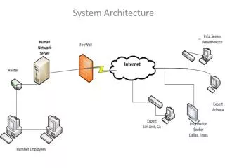
Pixel System Architecture 1 Sensor 16 Front End chips (FE) 1 Module Controller Chip (MCC) 2 VCSEL Driver Chips (VDC) 1 PIN diode receiver (DORIC) Module / stave Control room Optical Receivers (BOC) Readout Drivers (ROD) Readout Buffers (ROB) Timing Control (TIM) Slow Control, Supplies
Architecture Features (1) • Basic interface to the module outside uses 3/4-LVDS line protocol: • DCI: Data & Command InData and commands go to the MCC trough it. • DTO/DTO2: Data Out & Data Out 2DTO2 is used only in the B-layer to increase aggregate bandwidth • CK: 40 MHz clock synchronous with LHC operation • Basic interconnections between MCC and FE use serial protocol: • DAO: Data & Address Out (broadcast signal)Output from MCC to FE, serial bussed signal, full swing CMOS, 5 MB/s - not operate during data take • LD: LoadThis line distinguish between command/address (LD=0) from data (LD=1), bussed signal, full swing CMOS - not operate during data take • CCK: 5 MHz slow protocol clockSlow protocol validation clock used in together with DAO/LD and DTI<15:0>, bussed signal, full swing CMOS - not operate during data take • DTI<15:0> : Data InPoint-to point serial data link from FE’s to MCC, used both to read back configuration data from FE’s (in connection with DAO/LD/CCK) or to transmit events in response to LV1, LVDS (500µA).
Architecture Features (2) • Additional bussed signals to the FE’s are: • LV1: Level 1 TriggerLV1 is generated in response to a Trigger command received by the MCC. It is validated by XCK (module system clock). LVDS signal, bussed. • SYNC: ResetThe SYNC LVDS bussed signal issues resets to the FE’s. The width of the SYNC is linked to the reset hierarchy in the FE. • STRO: Calibration StrobeBussed LVDS signal used to inject a reference charge to the FE amplifiers. The rising edge of the STRO pulse can be delayed respect to XCK in 0.5 ns steps. • XCK: Module System Clock40 MHz system clock used for MCC/FE protocols. Fanout of the CK clock, LVDS. • Architecture is “data-push” style: each crossing for which LV1 accept is present causes all FE chips to autonomously transmit back hit information for the given crossing. LV1 signal may remain set for many contiguous crossings to allow readout of longer time intervals. MCC merges such events together.
MCC Architecture MCC basic functions: • FE & MCC configuration • Distribution of LV1 trigger to FE’s and record of L1ID and BCID of accepted LV1 triggres (PendingLv1FIFO - 16 words) • Collection of hits from FE’s, storing into ReceiverFIFO’s (16 FIFOs x 128 words), Event Build and serial transmission to the outside.
MCC Testability Features Part of silicon used to increase chip testability: • Scan chain: 3 pins for scan chain (TSTEN, TSTIN, TSTOUT). • Transparent Mode: single FE’s on the module accessed by transparent behaviour of the MCC (function dropped in the MCC-I1) • Event playback: events can be loaded in the MCC and reconstructed then by the MCC. • FIFOs & Registers R/W: all the memory structures in the MCC that can be written can be readout.
Chip Features: MCC-AMS • MCC-AMS uses 16 FIFO’s of 32 words each to store event hits from FE’s. • In the system architecture it needs a ladder/disk controller chip (LCC, never designed). • The STRO delay signal must be generated outside, the MCC-AMS only fans out the corresponding STRI (Strobe Input). • A “transparent-mode” is implemented in the chip that makes transparent the connection from the outside to the selected FE. Foreseen for initial debugging of a multi FE system. • Design methodology: • Verilog: behavioural description • Synergy: logical synthesys • Cell3 Ensemble: place & route • Clock distribution: Clock trunk with distributed parallel buffers (1 BUF x SC row)
MCC-AMS layout No. of SC: 17,922 No. of Trans.: layout = 416,464 schematics = 363,016 No. of Pins: 83 Chip Size: 10.6 x 6.3 = 66.8 mm2
Chip Features: MCC-D2 Changes from MCC-AMS: • Modified command set (to improve BER): Trigger command from 3 to 5 bits. • Redesign of command decoder state machines: no hidden states, from any state goes to idle. • Redesign of event data path and event building algorithm. • Full custom 16-bits x 16 words PendingLv1FIFO. • Programmable delay line for the STRO signal. • Second output line (DTO2) and selectable output data rate from 40 to 160 Mb/s.
MCC-D2 layout No. of Standard Cells: 13,446 No. of Transistors: 351,964 Chip size: 11.939 mm x 8.361 mm = 99.8 mm2 Full custom FIFO’s Delay Line Pending LV1 FIFO
Chip Features: MCC-I1 Changes from MCC-D2: • The ReceiverFIFOs depth increased to 128 words. • The PendingLv1FIFO created using a Synopsys macro library block. • The I/O pads, for use in the module, put on 3 sides of the chip. MCC-AMS pad compatibility kept by adding 10 additional pads. • Clock distribution uses balaced clock tree synthesised by CTGEN in Silicon Ensemble. • Power supply reduced from 3.3 to 2.0 V.
MCC-I1 layout No. of Standard Cells: 33,210 No. of Transistors: layout = 660,286 schematics = 627,972 Chip size: 6.380 mm x 3.980 mm = 25.4 mm2 Full custom FIFO’s Delay Line
Summary • Specifications for the Pixel system architecture defined in ‘97 with revision and back compatibility in ‘00. • First chip (MCC-AMS) produced in 1998 with radsoft modules built and operated from 1998 to 2001. • DMILL version of FE and MCC produced in 2000, no modules built due to low chip yield and insufficient rad tolerance. • First DSM chip versions produced in 2002. Both FE and MCC operated on detector modules successfully. Minor errors will be fixed for next submission.

