New Generation of Virtual Substrates
450 likes | 682 Vues
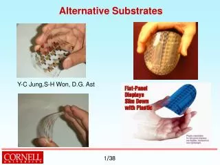
New Generation of Virtual Substrates. T. Grasby Dept. of Physics, University of Warwick. Device Layer. Si template (i.e. wafer). Si wafer. Straining Silicon with a Virtual Substrate. unstrained silicon. strained silicon (biaxial tensile). SiGe x(z). z. New template

New Generation of Virtual Substrates
E N D
Presentation Transcript
New Generation of Virtual Substrates T. Grasby Dept. of Physics, University of Warwick
Device Layer Si template (i.e. wafer) Si wafer Straining Silicon with a Virtual Substrate unstrained silicon strained silicon (biaxial tensile) SiGex(z) z New template (virtual substrate)
Why Global Strain? • Non, Non • Uniaxial process-induced strain more effective, more flexible • Riddled with defects • Expensive to produce
Why Global Strain? • GLOBAL STRAIN FOR EVER • Enables high (biaxial) stress levels ~ 0.9 GPa per 10% Ge concentration (y) • Comparably high uniaxial strain via patterning • Hybrid strain regime – global + process induced top-up • Platform for n-sSi/p-SiGe dual channel CMOS devices • Contender for 32-22nm node FDSOI • Needed for R&D on strained Ge devices • Route to Si-Ge-GaAs integration?
Big Questions is the quality there? is there a route to production?
First Generation VS (linear Ge grade) – Quality Issues Ge conc(y) ~ 20% - good for nMOS performance → threading (field) dislocation density (TDD) ≥ 105 cm-2 → pile-up densities (PUD) ~ 0.1 – 10 cm-1 → surface roughness ~ 1 – 3 nm involve CMP
Linear Grading – State of the Art RMS Field TDD TDD (cm-2) RMS roughness (nm) Pile-up TDD Germanium composition (%) From Y. Bogumilowiczet al., LETI and IQE
Linear Grading – State of the Art RMS Field TDD TDD (cm-2) RMS roughness (nm) Pile-up TDD Germanium composition (%) From Y. Bogumilowicz et al., LETI and IQE
Terrace Grading 20% Linear grade Ge Concentration 10% 0 8 2 4 6 Thickness (mm)
UK SiGe:C Epitaxy Centre SS-MBE MBE - V90S-ANT LP-CVD - ASM Epsilon 2000E ...from Lab to Fab GS-MBE/-CVD mode
Terrace Grading – development work (SS-MBE) 30% - 3 tier
Terrace Graded - TEM 60% 6 Tier
LG 30% ≈105 cm-2 TDD Pile-up ≈1 cm-1
Defect reveal in 104 cm-2 range TDD ≈ 4 x 104 cm-2
Defect Reveal in 103 cm-2 range LG 15%, 850ºC Pseudo Pile-up EPD = 6x10³
Hardly an etch pit in sight! Pile-up < 0.1cm-1 TD TDD ≈ 3x103 cm-2 PUD = 0
LG 40% TDD ≈ 106 cm-2 Pile-up ≈ 5cm-1
TG 40% TDD ≈ 3x105 cm-2 Pile- up = 0?
Terrace Grading – Elimination of Pile-ups?SiPHER Analysis TG (3 tier) up to 30% (SS-MBE) Photoluminescence image Surface image 6x6 mm area Pile-up density:≤ 0.1 cm-1 Measurements taken by Accent Optical Technologies near wafer centres
Terrace Grading – Elimination of Pile-ups?SiPHER Analysis 3 tier up to 30% (SS-MBE) TG LG Photoluminescence image Photoluminescence image Surface image 2x2 mm area Pile-up density: 3.5 - 6 cm-1 6x6 mm area Pile-up density:≤ 0.1 cm-1 Measurements taken by Accent Optical Technologies near wafer centres
What can Terrace Grading do? LG LG Terrace Grading ≡ Virtual CMP TG TG
30% Terrace Graded Properties(MBE growth) High T growth (850 790C) 3.5x10⁵ 2x10⁵
30% Terrace Graded Properties(MBE growth) High T growth + anneal + anneal 3.5x10⁵ 2x10⁵ 5x10³ 3x10⁵
30% Terrace Graded Properties(MBE growth) Low T growth 800 700C TG Low T + anneal 3.5x10⁵ 2x10⁵ 3x10³ 5x10³ 3x10⁵ 0 1.9
≈103 cm-2 TDD Pile-up < 0.1cm-1 30% TG TD TDD ≈ 3x103 cm-2 PUD = 0
Terrace Grading – (SS-MBE)TDD for y 50%High T growth - 850790C
Transfer to CVD • TG virtual substrates up to y = 0.2 grown on ASM Epsilon 2000E™ RP-CVD reactor using SiH4, SiCl2H2 and GeH4 precursors. • Optimisation work - growth temperatures, growth rates, strain gradients, no. of terraces, terrace widths, throughput, etc
Terrace Grading Properties (CVD) y→0.2 Reciprocal space maps (000 and 220) of 2 tier TG 20% sample taken with XRD AFM images showing 10x10μm area and 2x2μm area TD Typical etch pit image of TG sample capped with 10nm of strained silicon. TDD ~ 105
Pile-Up Free Photoluminescence image Surface image 6x6 mm area Pile-up density: 0 TG (2 tier) up to 17% (LPCVD) Measurements taken by Accent Optical Technologies
Misfits at the sSi/VS interface MD TD …….but tsSi = 10nm which is < tc (17nm)
EPD Reveal in VS with sSi layer Chemical etchant TD Strained silicon MD TD Virtual substrate Additional etch pit Etched surface 100% increase in EPD
Terrace Grading – basic studies (y→0.2)(with sSi layer)…CVD y 0.2 0.1 0.0 6 8 2 4 Thickness (μm) TDD (cm-2) Relaxation of upper terrace (%) Number of terraces
50% terrace graded (for sSi) TDD = 3x105 cm-2 PUD = 0
80% terrace graded (for sGe) TDD = 3x105 cm-2 PUD = 0
Terrace graded VSs – smoother! CMP LG data from LETI ….and no CMP
The Future • Terrace grading • Heralds a new generation in VS quality: • eliminates pile-up • low TDD • potential to avoid CMP • route to production√ • Current work • Examining new designs which directly manage the relaxation process: • → thinner virtual substrates • → TDD and PUD → zero • → smooth enough for wafer bonding • And finally • Still a lot of parameter space to be explored • – and if you thought Si-Ge relaxation was fully understood ..….……
Linkage with SiNANO • Many VS-based sSi layers supplied to WP1 and WP2 partners for device processing • VSs characterised by partners • VS-based sGe layers supplied to partner for device processing • VS-based sSiGe and sGe layers to be supplied to Jeulich for OI bonding trials • VS work enabled a presence on PULLNANO project