Outlook on Size-Scaling of Substrate-Transferred Crystalline Coatings Garrett D. Cole
Outlook on Size-Scaling of Substrate-Transferred Crystalline Coatings Garrett D. Cole Crystalline Mirror Solutions LLC / GmbH May 15, 2018. Outline. Quick background on Crystalline Mirror Solutions Overview of substrate-transferred crystalline coatings

Outlook on Size-Scaling of Substrate-Transferred Crystalline Coatings Garrett D. Cole
E N D
Presentation Transcript
Outlook on Size-Scaling ofSubstrate-Transferred Crystalline Coatings Garrett D. Cole Crystalline Mirror Solutions LLC / GmbH May 15, 2018
Outline • Quick background on Crystalline Mirror Solutions • Overview of substrate-transferred crystalline coatings • description of technological development and current status • Prospects for realizing GW-relevant crystalline coatings • discussion on the next steps for developing large-area optics
Spin-Off of Quantum Optomechanics Epitaxial AlGaAsmicro resonators Substrate-transferredcrystalline coatings multilayer GaAs/ AI0.92Ga0.08As fusedsilica free-standing epitaxial AlGaAs reflectivity >0.9999 (ppm losses) loss angle <4×10⁻⁵ to <5×10⁻⁶ crystalline coating a) Cole, et al., Appl. Phys. Lett. 92 (2008)b) Cole, Proc. SPIE. 8458–07 (2012) c) Aspelmeyer et al., RMP 86, 1391 (2014)
Global Footprint Vienna, Austria Zurich, Switzerland Custom coatings SantaBarbara, CA Standard coatings Optical testing Epitaxy CMS is rapidly growing, 16 total staff at 3 international sites
Substrate-Transferred Crystalline Coatings • Arbitrary substrate materials and geometries can be coated • SiO2, Si, SiC, Al2O3, YAG,YVO4, diamond, etc. • ROC > 10 cm • maximum diameter (limitedby GaAs wafer) of 20 cm • Key advantages over traditional IBS amorphous metal oxides • high mechanical Q • high thermal conductivity • high MIR transparency
Outline • Quick background on Crystalline Mirror Solutions • Overview of substrate-transferred crystalline coatings • description of technological development and current status • Prospects for realizing GW-relevant crystalline coatings • discussion on the next steps for developing large-area optics
Merging Semiconductors with Optics Monocrystalline GaAs/AlGaAs heterostructures grown on GaAs wafers by molecular beam epitaxy Using semiconductor manufacturing techniques, the multilayer is extracted from the original GaAs wafer Direct bonding is used to attach the single-crystal interference coating to the final optical substrate Epitaxial multilayers on arbitrary substrates
Epitaxial Coating Details Ø 5 mm • Ø 5 cm • AlGaAs multilayer with varying Al content for index contrast • high index layers consist of binary GaAs thin films • 8% Ga incorporated in low index AlGaAs layers to slow oxidation in ambient • Potential for ppm-level optical losses from ~900 nm → 4+ μm • peak performance in NIR • High quality epitaxy requires a lattice matched substrate • same crystalline symmetry • minimal deviation of lattice parameter (atomic spacing) Maximum coating diameterlimited by GaAs growth wafer (currently up to 20 cm), widevariety of substrates possible G. D. Cole, W. Zhang, M. J. Martin, J. Ye, and M. Aspelmeyer, Nature Photonics (2013)
Ultrastable Optical Reference Cavities • Dozens of cavities deployed using silica, silicon, and sapphire subs. • Mirror diameters of 0.5” to 1” and spacer lengths up to 30 cm • Wavelengths from ~1000 nm to 1600 nm, RT and cryo (4-124 K) • cavity finesse exceeding 600,000 (<3 ppm S+A) measured via ringdown
Size Scaling of Crystalline Coatings • Optomechanical performance of crystalline coatings has been proven at the 1” scale • 20-cm diameter coatings possible now in principle • aLIGO test masses are 35 cm in diameter with demanding coating specifications • < 1 ppm absorption • scatter at the < 10 ppm level • thickness variation < 1%(trans. variation < 1 ppm) Can we maintain the excellent performance of crystalline coatings at LIGO-relevant size scales?
AEI “SQL Optics” Effort 24 mm 48 mm 10-m prototype • High-performance ~50-mm diameter optics for the 10-m Prototype • small-scale test bed for advanced interferometer technologies • similar rigorous performance requirements as with the larger systems • Can we meet the desired properties with reasonable yield? • absorption < 3 ppm, scatter < 10 ppm, uniformity < 1 nm RMS
Test Coating Runs 2016/2017 • High reflectivity 1064 nm crystalline coatings on fused silica wafers • 35.5 period mirror, target transmission of 10 ppm at normal incidence • Samples used for process evaluation and in-depth characterization • properties of interest include optical scatter and thickness uniformity
2” Optics Testing, NAOJ / LMA STICK AROUND FOR MANUEL MARCHIÒ’S TALK! Marchio et al., Optics Express, vol. 26, no. 5, 6114 (2018)
Compiled Performance Metrics • Substrate-transferred crystalline coatings simultaneously exhibit excellent optical and mechanical quality • Loss angle reduction of 10-100×compared with IBS • IBS-deposited Ta2O5/SiO2: φIBS ≈ 2×10⁻⁴ • AlGaAs room temperature: φRT <4×10⁻⁵ • AlGaAs cryogenic performance: φcryo <5×10⁻⁶ • Minimal scattering loss and optical absorption • absorption verified at < 1 ppm, scatter loss < 3 ppm (mm spot) • large-area scatter and thickness uniformity comparable to IBS • Thickness uniformity and optical scatter meet specs. • only financial barriers remain for producing LIGO-scale coatings
Outline • Quick background on Crystalline Mirror Solutions • Overview of substrate-transferred crystalline coatings • description of technological development and current status • Prospects for realizing GW-relevant crystalline coatings • discussion on the next steps for developing large-area optics
Scalable Production Technique • Leverage semiconductor infrastructure for LIGO-scale optics • high-uniformity epitaxial growth on large-diameter substrates • void-free direct bonding of crystalline semiconductors • commercial tools available for LIGO-relevant mirror sizes
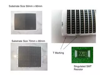
Scalable Production Technique Bonding: 45 cm GaAs wafers: 20 → 40 cm Epitaxy: 30 → 40 cm • Crystalline coatings limited to ⌀20 cm, three areas to scale • commercial GaAs wafers currently available up to 20-cm diam. • epitaxy qualified for wafer sizes of 30 cm (~50-cm chamber diam.) • semiconductor direct bonding demonstrated to diam. of 45 cm
LIGO-Scale GaAs Wafers • Promising discussions with Freiberger Compound Materials • currently produce GaAs wafers up to 20-cm diameter • VGF crystal growth capabilities up to ~40-cm max diameter • “waferizing” processes must be scaled up (main cost driver) • Estimated 2 year timeline and total cost of ~$5M
Step 2: LIGO-Scale Epitaxy • Ongoing discussions with external epi foundries (US based) • two options for production MBE reactors: • Veeco Gen2k or Riber7000/8000 • LIDAR and facial recognition is rapidly changing market • Estimated 3-4 year timeline and total cost of ~$7M-10M
Step 3: LIGO-Scale Bonding • Electronic Visions Group, key vendor for semicon. bonding • currently offer a production tool for 45-cm SOI manufacturing • SOI: silicon on insulator, wafers for microwave electronics • designed for 1-mm thick subs., must be modified for optics • Estimated 3-4(?) year timeline and total cost of ~$10M Si SiO2 Si
Large-Area Coating R&D Efforts Quantum Measurement Enhanced Gravitational wave detection (Q-GWD) GRANTED, Timeline: 08/2017–11/2020 • total value of 1.948 k€, 663 k€ for CMS • scaling of crystalline coatings to 200 mm in diameter • development of a non-classical laser source for quantum-enhanced GWD by the Niels Bohr Institute (Polzik group), DanmarksNationaleMetrologiinstitut, and Therkildsen Development ApS (Denmark) European Quantum Technologies Network for Gravitational Wave Astronomy (QGRAV) SUBMITTED, 3 year timeframe if successful • H2020 quantum flagship, value of 3.8 M€, (240 k€ CMS) • consortium of 12 academic and 4 industry partners • development of quantum-enhanced detection technologies applicable to gravitational-wave detectors • demonstration of >200-mm diameter crystalline coatings 48-mm diameter10-m prototype optic (Hannover)
Thanks from Everyone at CMS! CMS Confidential