Efficient Error-Cancelling Algorithmic ADC: Revolutionizing High-Resolution Conversion
This presentation focuses on an innovative algorithmic Analog-to-Digital Converter (ADC) designed for medium-speed, high-resolution applications. By reducing the clock periods required for bit conversion from seven to just four, the new technique enhances efficiency and performance. Key aspects include manipulating capacitor switching for accurate residue amplification, leading to significant improvements in Signal-to-Noise and Distortion Ratio (SNDR) from 57 dB up to 90 dB. The ADC is set to operate at 1.8 V, sampling at 100 kHz with a 16-bit resolution, while consuming only 4 mW of power.

Efficient Error-Cancelling Algorithmic ADC: Revolutionizing High-Resolution Conversion
E N D
Presentation Transcript
EFFICIENT ERROR-CANCELLING ALGORITHMIC ADC Adviser: Dr.Hsun-hsiang Chen Presenter : Chieh-En Lo
OUTLINE • Introduction • Converter structure • Accurate residue amplification • Simulation results
INTRODUCTION • medium-speed high-resolution • Most recent technique that uses a minimum of 7 clock periods per bit conversion, all tasks in the new technique is accomplished in 4 clock periodsper bit. • The key concept is to manipulate the switching of capacitors.
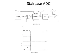
CONVERTER STRUCTURE V(k+1) = 2V(k)+b(k)Vref
SNDR can be improved from 57db to 90db. • The proposed ADC is being designed and fabricated to achieve 1.8 V, 100 ksample/s and 16 bit resolution with 0.18 pm double-poly CMOS process. The expected active area is about 600 um x 700um, and the expected power consumption is about 4 mW