Asynchronous interface
This article provides an in-depth look at RS-485 and IIC interfaces, exploring their functionalities, advantages, and ideal applications in various communication systems. RS-485 is highlighted for its capacity to connect up to 256 devices over long distances at high speeds, making it a cost-effective and efficient option for robust networking. Meanwhile, the IIC, or I²C interface, is examined for its synchronous communication capabilities and multi-master support, detailing its uses in peripherals like sensors, LCD drivers, and audio processors. Discover how these interfaces enhance modern technology.

Asynchronous interface
E N D
Presentation Transcript
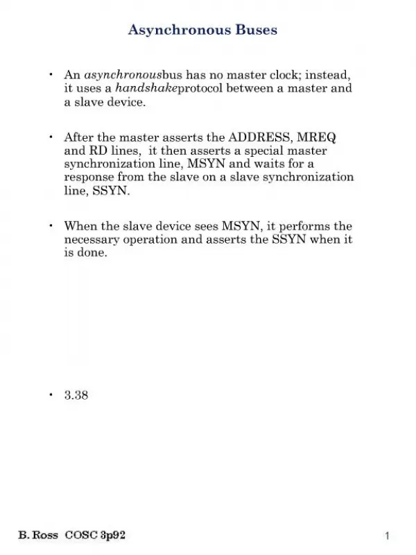
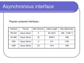
Asynchronous interface Popular computer interfaces :
Synchronous Interface Popular computer interfaces :
About RS-485 • When you need to transmit over long distances or at higher speeds than RS232 can handle, RS-485 is a solution. • Another advantage is that the RS-485 link is not limited to just two devices. • Depending on the distance, bit rate, and interface chips, as many as 256 nodes can be connected along a single pair of wires. • RS-485 is the interface described by a document titled TIA/EIA-485. A similar standard is ISO/IEC 8482.1993.
RS-485 advantages over RS2-32 • Low cost: Driver & receivers are inexpensive and require just a single +5V supply to generate the required minimum 1.5V difference at the differential outputs. • Networking ability: Instead of being limited to two devices, RS-485 is multi drop interface that can have multiple drivers and receivers. With high impedance receivers, an RS-485 link can have as many as 256 nodes. • Long Links: A RS-485 link can be as long as 4000 Feet as compared to RS-232’s typical limit of 50 to 100 feet. • Speed: The bit rate can be as high as 10Mega Bits/Second. The cable length and the bit rate are related. Lower bit rates allow longer cables.
Balanced & Unbalanced lines • The main reason why RS-485 can transmit over long distances is because it uses balanced lines. Each signal has a dedicated pair of wires, with the voltage on one wire equal to the negative, or complement, of the voltage on the other. The receiver responds to the difference between the voltages. A big advantage to balanced lines is their immunity to noise. This is also called differential signaling. • In contrast, RS 232 uses unbalanced or single ended lines. The receiver responds to the difference between a signal voltage and a common ground used by all systems. An unbalanced interface may have multiple ground wires, but all of the signal grounds connect together. • TIA/EIA-485 designates the two lines in a differential pair as A and B. At the driver, a TTL logic-high input causes line A to be more positive than line B, while a TTL logic low input causes line B to be more positive than A.
Schematic representation At the receiver if input A is more positive than input B, the TTL output logic is high and if the input B is more positive than input A , the TTL output is low logic.
Why balanced lines are quiet • Balanced lines are quiet because the two signal wires carry nearly equal, opposite currents. • This reduces received noise because most noise voltages are present more or less equally on both wires. • A balanced receiver sees only the transmitted signal, with noise eliminated or very much reduced. • Another advantage to balanced lines is that they are immune, within limits, to differences in ground potential between the driver and receiver. • In a long link, the grounds at the driver and receiver may vary by many volts. • A balanced line doesn't care about mismatched grounds, because the receiver detects only the difference between the two transmitted signals.
Synchronous Communication IIC SPI
Some IIC devices • I/O Expander devices. • LCD & LED driver devices. • Video controller. • PAT/NTSC TV processors • TV and VTR stereo/dual sound processors with integrated filters. • Hi-Fi stereo audio processor interface for color decoder. • YUV/RGB switches. • Programmable modulators for negative-video modulation and FM sound. • Satellite sound receiver. • 1.4 GHz multimedia synthesizer.
IIC Interface Principals • IIC is a synchronous serial bus developed by Phillips to allow communication between different peripherals. • Many devices such as EEPROMs, ADCs, LCD drivers, DACs etc support IIC protocol. • The devices on the bus communicate through a two wire interface. Typical data transfers are 100Kbits/Sec, 400Kbits/Sec and even 1Mbit/Sec. • The number of devices on the bus is limited by the maximum bus capacitance of 400pF. • Most devices are used as slaves while the microcontrollers are typically masters. • IIC also supports multi-mastering, which means more than one device is allowed to control the bus. • IIC has collision detection and arbitration to maintain data integrity.
IIC protocol • IIC is a multi-master/slave protocol. All devices connected to the bus must have an open-collector or open drain output. • A transaction begins when the bus is free (ie. both SCL and SDA are high). • A master initiates a transfer by generating a START condition. The master then sends an address byte that contains the slave address and the transfer direction. • The addressed slave device must acknowledge the master. If the transfer direction is from master to slave, the master becomes the transmitter and writes to the bus. • The slave becomes the receiver and reads the data and acknowledges the transmitter and vice-versa. • When the transfer is complete, the master sends a stop condition and the bus becomes free. In both transfer directions; the master generates the clock SCL and the START/STOP conditions.
The START condition is generated by a high to low transition on the SDA line during the High period of SCL line. • A STOP condition is generated by a low to high transition on the SDA line during the High period of the SCL line. • The number of bytes transferred per START/STOP frame is unrestricted. • DATA bytes must be 8-bits long with the most significant bit (MSB) first. • Each valid data bit sent to the SDA line must remain high for “1” or low for “0” during the high period of the SCL, otherwise any transition in the SDA line while SCL is high will be read as START/STOP condition. • Transitions can only be made during low period of SCL. • An acknowledgement bit must follow each byte. After the last bit of the byte is sent, an ACK clock (acknowledgement clock) is generated by the master (9th Clock). An ACK (acknowledge bit, low) must be sent by the receiver and remain low during the high period of the ACK clock.
If the slave (receiver) doesn’t return an ACK (e.g an error, or is unable to receive data), then the slave device must leave the SDA line high (NACK). • The master will abort transmission by generating a STOP condition. • The slave will need to keep the SDA line high for the master to generate the STOP condition. • If the receiver is the master and the transfer is ending then, the master needs to send NACK. The slave ( now transmitter) must release the SDA line to high, this allows the master to generate a START/STOP condition. • At the beginning of each transfer, the master generates the START condition, then sends a slave address. The standard slave address is 7 bit (sometimes 10 bit) followed by a direction or R/W bit (8th bit). • When the direction bit is a WRITE (zero), the addressed slave becomes the receiver and the master is the transmitter. When the direction bit is a READ (one), the addressed slave device becomes the transmitter and the master becomes the receiver.
Arbitration • A master may transfer only if the bus is free. Two or more masters may generate a start condition within the minimum hold time of the start condition. This results in a defined START condition to the bus. • Arbitration takes place on the SDA line, while SCL line is at high level. One master transmits a high level, while another master is transmitting a low level. The second master will switch off its DATA output stage because the level on the bus doesn’t correspond to its own level. • Arbitration can continue for many bits. Its first stage is comparison of the address bits. If the masters are each trying to address the same device, arbitration continues with the comparison of the data-bits. Address and data information on the IIC bus is determined by the winning master, no information is lost during the arbitration process. • A master that loses the arbitration can generate clock pulses until the end of the byte in which it loses the arbitration.
Arbitration procedure of two masters If a master also incorporates a slave function and it loses arbitration during the addressing stage, it's possible that the winning master is trying to address it. The losing master must therefore switch over immediately to its slave mode. The moment there is a difference between the internal data level of the master generating DATA 1 and the actual level on the SDA line, its data output is switched off, which means that a HIGH output level is then connected to the bus. This will not affect the data transfer initiated by the winning master.
Since control of the IIC-bus is decided solely on the address or master code and data sent by competing masters, there is no central master, nor any order of priority on the bus. • Special attention must be paid during a serial transfer,if the arbitration procedure is still in progress at the moment when a repeated START condition or a STOP condition is transmitted to the IIC-bus. such a situation to occur, the masters involved must send this repeated START condition or STOP condition at the same position in the format frame. • In other words, arbitration isn't allowed between… • A repeated START condition and a data bit • A STOP condition and a data bit • A repeated START condition and a STOP condition. Slaves are not involved in the arbitration procedure.
Possible data transfer formats • Master-transmitter transmits to slave-receiver. The transfer direction is not changed . • Master reads slave immediately after first byte. At the moment of the first acknowledge, the master- transmitter becomes a master- receiver and the slave-receiver becomes a slave-transmitter. This first acknowledge is still generated by the slave. The STOP condition is generated by the master, which has previously sent a not-acknowledge.
Combined format. During a change of direction within a transfer, the START condition and the slave address are both repeated, but with the R/W bit reversed. If a master receiver sends a repeated START condition, it has previously sent a not-acknowledge.
Definition of bits in the first byte • The addressing procedure for the IIC-bus is such that the first byte after the START condition usually determines which slave will be selected by the master. • When an address is sent, each device in a system compares the first seven bits after the START condition with its address. If they match, the device considers itself addressed by the master as a slave-receiver or slave-transmitter, depending on the R/W bit.
A slave address can be made-up of a fixed and a programmable part. Since it's likely that there will be several identical devices in a system, the programmable part of the slave address enables the maximum possible number of such devices to be connected to the IIC-bus. The number of programmable address bits of a device depends on the number of pins available. • The IIC-bus committee coordinates allocation of IIC addresses.
Introduction • SPI was developed by Motorola semiconductors. SPI uses a master-slave model and typically has three signal lines: data input line, data output line and clock line. • Chip select signals from the master are used to address different slaves on the bus. The hardware realization of such an interface is a simple shift register. • The data bits are shifted in/out MSB (most significant bit) first. Often the data is shifted simultaneously out from the output pin and into the input pin. • SPI interface defines only the communication lines and the clock edge, other parameters vary for different devices. Clock frequencies happen to be anywhere from 100kHz to a few MHz and word lengths are from 8 to 16 or more bits.
Signal Description • 4 basic signals… MOSI, MISO SCLK SS
MOSI, MISO,SCLK, SS • Master Out, Slave In : An output line from master device and input into slave device. MOSI line transfers data in one direction only from Master to Slave. • Master In Slave Out : An input line into the master device and output from slave device. MISO line transfers data in opposite direction in MOSI line, i.e. transfers data from a slave to master device. • Serial Clock : SCLK line used to synchronize both, data in and out of a device via MOSI, MISO lines. SCLK generated by master. Hence is input to all slave devices. • Slave select : SS lines are controlled by master to select slave device. Must be low prior to data transaction and must stay low for duration of transaction. Each slave device requires its own SS input line from the master. In slave device logic low received on SS line and clock input at SCLK pin. This synchronizes slave with the master. Data then is received serially at MOSI. During write cycle data shifted on to MISO pin on clock from master.
SPI Operation • To initiate data transfer SS line must go low. This synchronizes the slave device with master. Data can be transferred between the master and slave in one of the two modes… • Data sampled at the raising edge of the clock • Data sampled on the falling edge of the clock.
Features • Full duplex, three-wire synchronous transfers • Clock rate selectable up to 1.72MHz (2.5MHz possible with slight • modifications) • Master send frequency adjustable up to 1.72 MHz • Slave receive frequency adjustable upto 1.1 MHz • Word length selectable anywhere from 1-16 bits. • (More than 16 bits easily implemented if required) • Clock polarity is configurable by using the appropriate command byte • This multimode capability combined with simple shift register architecture makes the SPI bus very versatile. • Due to this versatility many non-SPI serial devices including most shift registers may be used as SPI slaves.
Clock Modes • All data transferred by serial clock. • 1 Bit of data is transferred for each clock cycle • 4 versions of clock to data relationship are defined for the SPI bus. • These versions, Mode A thru D are determined by value of clock polarity (CPOL) and clock phase (CPHA) bits. • Any hardware device capable of operating in more than one mode will have some means of selecting the value of these bits. • Clock polarity determines the level of clock idle state and clock phase determines which clock edge places new data on the bus. • Mode required for a given application generally determined by slave.
Clock Polarity CPOL • If CPOL cleared (logic 0) and no data is being transferred (idle state), the master holds SCK line low. If CPOL is set (logic 1) master idles the SCK line high.
Clock Phase CPHA • CPHA, in conjunction with CPOL, controls when data is placed on the bus (shifted out). If CPHA is set (logic 1) data shifted out on to MOSI line determined by the value of CPOL. • For CPHA set if CPOL is set new data is placed on the line at the down going clock and is read at the up going clock. • IC CPOL is cleared, new data is placed on the line at the up going clock and is read at the down going clock. • IF CPHA is cleared (logic 0) the shift clock is the OR of the SCK with SS. As soon as SS goes low, new data is placed on the line and the first edge of the clock reads the data. • IF CPOL is set the first clock edge is down going and subsequent data bits are read at each down going clock. Each new bit is placed on the line at the up going clock. • IF CPOL is cleared the first clock edge is up going and subsequent data bits are read at each up going clock. Each new bit is placed on the line at the down going clock.
Interfacing USB A Practical Implementation Chip Solutions Microcontrollers with on-chip USB Hardware
A Practical Implementation… • Interfacing current generation printers • Adding extended memory (USB Pen drive) • Adding USB peripherals like modem’s etc A synchronous two wire communication interface employing differential signaling technique, with hot plug in capabilities & device recognition. (MAX number of devices 127) USB interface available in slow speed & High speed, USB (1.1 --- 1.5MBps) & USB (2.0 --- 12Mbps).
Electrical Specifications: USB Transfers signal & power over a 4 wire cable. The actual communication is effected between (D+) & (D-), two wires and point to point segments. The signals on each segment are differentially driven into a cable of 90Ω intrinsic impendence. The clock is transmitted encoded along with the differential data. The clock encoding scheme is NRZI (Non Return to Zero Inverted) with bit stuffing to ensure adequate transitions. A SYNC field precedes each packet to allow the receiver (s) to synchronize their bit recovery clocks. In order to provide guaranteed input voltage levels and proper termination impedance, biased terminations are used at each end of the cable. The terminations also permit the detection of attach and detach at each port and differentiate between full speed and low speed devices.
BUS PROTOCOL: Bus transactions involve the transmission of up to three packets. Each transaction begins when the host controller, on a scheduled basis, sends a USB packet describing the type and direction of transaction, the USB device address, and endpoint number. This packet is referred to as the Token Packet. The USB device that is addressed selects itself by decoding the appropriate address fields. The source of the transaction then sends a Data Packet or indicates it has no data to transfer. The destination in general responds with a Handshake Packet indicating whether the transfer was successful.
The USB data transfer model between a source or destination on the host and an endpoint on a device is referred to as a pipe. There are two types of pipes: stream and message. Stream data has no USB defined structure while message data does. Additionally, pipes have associations of data bandwidth, transfer service type, and endpoint characteristics like directionality and buffer sizes. Devices on the USB are physically connected to the host via a tiered star topology. USB attachment points are provided by a special class of USB device known as a hub. The additional attachment points provided by a hub are called ports. A host includes an embedded hub called the root hub.
Most-relevant USB classes … • Mass Storage Device (MSD), • Human Interface Device (HID), • Device Firmware Upgrade (DFU), • Communication Device Class (CDC), • One of the major advantages of HID is that you do not need to supply a custom driver, as one is already supplied with the operating system. A limitation of HID is that its data transfer rate is limited to a maximum of 64KB per second. However, this is still significantly faster than RS-232 (115200 baud is approximately 12KB per second). In addition, modern embedded system designs are now using the USB Bus to connect a device to a PC, rather than a legacy system such as RS-232. On the other hand CDC, is a virtual comport implementation and can be read & written to as that of any standard PC Serial port.
Physical Bus Topology Devices on the USB are physically connected to the host via a tiered star topology. USB attachment points are provided by a special class of USB device known as a hub. The additional attachment points provided by a hub are called ports. To prevent circular attachments, a tiered ordering is imposed on the star topology of the USB. This results in the tree-like configuration
PIC 18F4550 • PIC Devices with USB… • 18F4550
ATMEL AVR Devices The following devices have USB interface for applications needing to communicate with USB host. AT90USB82: 8KB FlashAT90USB162: 16KB FlashAT90USB646: 64KB FlashAT90USB1286: 128KB Flash The following devices comply with the USB On-The-Go (OTG) standard for use as Dual Role Devices (DRD) in applications operating as either host or function on the USB. The USB host capability is key to embedded devices needing to communicate without PC intervention. AT90USB647: 64KB FlashAT90USB1287: 128KB Flash