Download
1 / 31
310 likes | 325 Vues
Learn about microarchitecture, storage elements, combinatorial logic, clock signals, and design processes in digital systems.

E N D
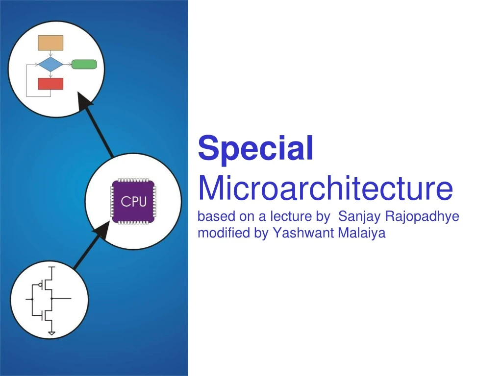
SpecialMicroarchitecturebased on a lecture by Sanjay Rajopadhyemodified by Yashwant Malaiya
Computing Layers Problems Algorithms Language Instruction Set Architecture Microarchitecture Circuits Devices
LC-3 Data PathRevisited Filled arrow = info to be processed. Unfilled arrow = control signal.
Microarchitecture • Functional hardware blocks in a digital system • Storage: Registers, Register file, Memory • Triggered by the system clock • Combinational: MUXes, ALU, adder, SEXT, wiring etc. • Respond after some propagation delay Design process: • Design the data path and identify control signals • Design the Control finite state machine
Timing relative to system clock • Combinational blocks (Logic and wiring) • Output is always a function of the values on input wires • If input changes, the change propagates with some propagation delay. • Storage elements are timed • Clock – a special signal that determines this timing • Storage can be updated only at the tick of the clock • What happens between ticks? • The “current” values are processed by logic and wiring to produce values … • … that will be used to update at the “next tick” • How fast can the clock tick? • Must allow for the longest combinational signal path
Timing relative to system clock • How fast can the clock tick? • Must allow for the longest combinational signal path. • Clock frequency: tick rate • Ex: 2 GHz mean 2x10⁹ cycles per second • Clock period: period between two pulses • Inverse of clock frequency • 2 GHz clock frequency means period is 0.5 nanosecond clock period. • Signals must stabilize between two clock periods. Thus longest combinational signal path must be less than a clock period.
Register Transfer and Timing • In one clock period, signals travel from a source register(s) to a destination register, through the combinational logic. • Register transfer notation describes such transfer. For example: • Reg[1] Reg[1] + Reg[2] • Condition is the logical condition for which this transfer takes place (often in terms of control signals). • Transfer takes one clock cycle. Memory operations assumed here to take one cycle also • In reality memories are slow, and take multiple cycles • Register transfer languages: • Basic: here • Advanced: VHDL, Verolog: used for description/design
Combinational Logic • A digital circuit that computes a function of the inputs. Examples: • Adder: takes X and Y and produces X + Y • AND: takes X and Y, produces bitwise and • NOT: takes X and Y and produces ~X • 2-to-1 MUX: takes three inputs, X, Y and s (the last one is 1-bit) and produces (note that this is C-syntax, not the RTN that we will show later) (s==0) ? X : Y
Multiplexer (MUX) - refresher • n-bit selector and 2n inputs, one output • output equals one of the inputs, depending on selector Functional representation 4-to-1 MUX
Wires and Busses • Wires are (almost) just like electrical wires • Directional (arrows), sometimes bidirectional • May have a “thickness:” number of bits of data: e.g., the adder output is 16-bits in LC-3 • Busses: • Shared wires • Anyone can read at all times • Write is via arbitration (control signals to decide who gets to write on the bus)
Storage Elements • Large scale storage (memory): view it like an array • Address, Data in/out • Small scale storage (registers): • Programmer-visible registers: R0 … R7 • Special purpose registers: • PC, IR, PSR (processor status register), MAR, MDR
Register - refresher • A register stores a multi-bit value. • We use a collection of D-latches, all controlled by a common WE. • When WE=1, n-bit value D is written to register.
Memory • Processor issues commands to memory, who responds • Mem.EN(memory enable): hey, I’m talking to you • Mem.RW: here’s what I want you to do • Two special registers • Memory Address Register (MAR): only processor writes to this • Memory Data Register (MDR): both processor/memory can write to this • the processor generates the control signals • If Mem.EN and • if Mem.RW==0, (i.e.., read) the memory outputs the value at address MAR, • If Mem.RW==0, copy the contents of MDR into location Mem[MAR]
Registers Every register is connected to some inputs and has a special “load” signal. • If load signal is 1 at the next clock tick the input is stored into the register • Otherwise, no change in register contents (LD.PC & (PCMux = 10) ) ? PC PC+1 In terms of simple RTN notation PC PC+1 Which assumes that during the cycle [LD.PC & (PCMux = 10)) is true.
Data Path Components • Global bus • special set of wires that carry a 16-bit signal to many components • inputs to the bus are “tri-state devices,”that only place a signal on the bus when they are enabled • only one (16-bit) signal should be enabled at any time • control unit decides which signal “drives” the bus • any number of components can read the bus • register only captures bus data if it is write-enabled by the control unit • Memory • Control and data registers for memory and I/O devices • memory: MAR, MDR (also control signal for read/write)
Data Path Components • ALU • Accepts inputs from register fileand from sign-extended bits from IR (immediate field). • Output goes to bus. • used by condition code logic, register file, memory • Register File • Two read addresses (SR1, SR2), one write address (DR) • Input from bus • result of ALU operation or memory read • Two 16-bit outputs • used by ALU, PC, memory address • data for store instructions passes through ALU
Data Path Components • More details later. • Multiplexer (MUX): selects data from multiple sources • PC and PCMUX • Three inputs to PC, controlled by PCMUX • PC+1 – FETCH stage • Address adder – BR, JMP • bus – TRAP (discussed later) MAR and MARMUX • Two inputs to MAR, controlled by MARMUX • Address adder – LD/ST, LDR/STR • Zero-extended IR[7:0] -- TRAP (discussed later)
Data Path Components • Condition Code Logic • Looks at value on bus and generates N, Z, P signals • Registers set only when control unit enables them (LD.CC) • only certain instructions set the codes(ADD, AND, NOT, LD, LDI, LDR, LEA) • Control Unit – Finite State Machine • On each machine cycle, changes control signals for next phaseof instruction processing • who drives the bus? (GatePC, GateALU, …) • which registers are write enabled? (LD.IR, LD.REG, …) • which operation should ALU perform? (ALUK) • … • Logic includes decoder for opcode, etc.
Register Transfer Notation • Compact, “program-like” notation • Describe what happens in the datapath • One or more transfers per clock tick • one line = one clock tick • Two columns: • Write the desired transfers • List control signals to “effect the transfer” • LC3-Viz is a handy tool • LC3 Visualizer
RTN/LC3-Viz Conventions • Signals indicated must be asserted before the clock tick in order for the indicated transfer to occur. Sequence is: • Signals are asserted • Clock tick arrives, and causes the transfer • In an RTN transfer, on either the right hand side (rhs), or left hand side (lhs) • Mem[x] is the memory at address x • Mem[MAR] is the memory at address that is in the MAR • Reg[x] is Register number x
RTN Conventions • An RTN transfer is of the form: LHS-location RHS-expression • The LHS-location may be a memory or a specific register or the xth register • The RHS-expression is: • named registers, e.g., Reg[3] • memory locations e.g., Mem[MAR] • simple expressions PC+1, Reg[src] + Reg[dst]
How does the LC-3 fetch an instruction? • # Transfer the PC into MAR • Cycle 1: MAR PC; PC PC+1 # LD.MAR, GatePC, LD.PC, PCMUX • # Read memory; increment PC • Cycle 2: MDR Mem[MAR] # LD.MDR, MDR.SEL, MEM.EN • # Transfer MDR into IR • Cycle 3: IR MDR # LD.IR, GateMDR
Control Unit State Diagram • The control unit is a state machine. Here is part of asimplified state diagram for the LC-3: A more complete state diagram is in Appendix C. It will be more understandable after Chapter 5.
Control Unit State Diagram Appendix C.
How does the LC-3 decode the instruction? • # Special decode step (controller makes decision, no clock cycle is wasted since it only involves logic) • # No visible signal is active
How does the LC-3 execute a NOT instruction? • # Src register contents are negated by ALU and result is stored in dst register • Cycle 4: DR ~SR1; CC Sign(~SR1) • # LD.REG, DR, GateALU, ALUK, SR1, LD.CC
Other instructions • Every instruction is a sequence of transfers • Every instruction has the same first three cycles - Instruction fetch • Every instruction takes (at least one) additional cycle - Some take even more more • Each one effected by a specific set of control signals • The Controller is responsible for generating the correct signals in the appropriate cycle • Reminder - Logic responds after some propagation delay, - Storage loads are on clock ticks