The Microarchitecture Level
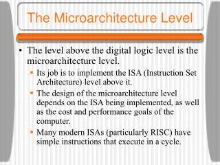
The Microarchitecture Level. The level above the digital logic level is the microarchitecture level. Its job is to implement the ISA (Instruction Set Architecture) level above it.

The Microarchitecture Level
E N D
Presentation Transcript
The Microarchitecture Level • The level above the digital logic level is the microarchitecture level. • Its job is to implement the ISA (Instruction Set Architecture) level above it. • The design of the microarchitecture level depends on the ISA being implemented, as well as the cost and performance goals of the computer. • Many modern ISAs (particularly RISC) have simple instructions that execute in a cycle.
The Microarchitecture Level • More complex ISAs (such as the Pentium II) require many cycles per instruction. • Executing the instruction may require: • locating the operands in memory • reading them • storing the results back into memory • The sequencing of operations within a single instruction often leads to a different approach to control than for simple ISAs.
An Example Microarchitecture • We will now show an example microarchitecture level based on a subset of the Java Virtual Machine ISA. • The subset contains only integer operations and is called the IJVM. • IJVM has some relatively complex instructions. • Many such architectures have been implemented through microprogramming. • The microarchitecture will contain a microprorgam (in ROM), whose job is to fetch, decode, and execute IJVM instructions.
An Example Microarchitecture • We can think of the design of the microarchitecture as a programming problem, where each instruction of the ISA level is a function to be called by a master program. • In this model, the master program is a simple, endless loop that determines a function to be invoked, calls the function, then starts over. • The microprogram has a set of variables called the state of the computer, that can be accessed by all the functions.
An Example Microarchitecture • Each function changes at least some of the variables making up the state. • For example, the Program Counter (PC) is part of the state. It indicates the memory location containing the next function to be executed. • During the execution of each instruction, the PC is advanced to point to the next instruction to be executed. • Each IJVM instruction has a few fields, usually one or two. The first field of every instruction is the opcode. Many instructions have an additional field, which specifies the operand.
The Data Path • The data path is that part of the CPU containing the ALU, its inputs, and its outputs. • The registers at the microarchitecture level are accessible only at that level. • Most registers can drive their contents onto the B bus. • The output of the ALU drives the shifter and the C bus, whose value can be written into one or more registers at the same time. • There are six ALU control lines.
The Data Path • F0 and F1 determine the ALU operation. • ENA and ENB individually enable the inputs. • INVA inverts the left input • INC adds 1 to the result. • Not all 64 combinations of input lines do something useful, however. • The ALU needs two data inputs: a left input (A) and a right input (B). Attached to the left input is a holding register, H. Attached to the right input is the B bus, which can be loaded from any of the nine sources.
The Data Path • H can be loaded initially by choosing an ALU function that just passes the right input (from the B bus) through to the ALU output. • For example, add the ALU inputs, but with ENA negated. • Two other control lines can be used independently to control the output from the ALU. • SLL8 (Shift Left Logical) shifts the contents left by 1 byte, filling the 8 least significant bits with 0s.
The Data Path • SRA1 (Shift Right Arithmetic) shifts the contents right by 1 bit, leaving the most significant bit unchanged. • It is explicitly required to read and write the same register on one cycle since reading and writing are done at different times within the cycle. • The timing of the events in a cycle is shown in the next slide. • A short pulse is derived from the main clock. • The subcycles can best be thought of as being implicit.
Memory Operation • The machine has two different ways to communicate with memory: • a 32-bit word-addressable memory port • an 8-bit, byte addressable memory port • The 32-bit port is controlled by two registers, MAR (Memory Address Register) and MDR (Memory Data Register). • The 8-bit port is controlled by one register, PC, which reads 1 byte into the low-order 8 bits of MBR. The port can only read memory from data, not write.
Memory Operation • Each of these registers is driven by one or two control signals. • An open arrow under a register indicates a control signal that enables the register’s output onto the B bus. • A solid black arrow indicates a control signal that writes the register from the C bus. • MAR contains word addresses. • PC contains byte addresses. • In the actual physical implementation, there is only one real memory and it is byte oriented.
Memory Operation • When MAR is placed on the address bus, its 32 bits do not map onto the 32 address lines, 0-31, directly. • Instead MAR bit 0 is wired to bus line 2, MAR bit 1 to 3, etc. • The upper 2 bits of MAR are discarded since they are needed only for word addresses above 232 which are illegal on our 4-GB machine. • When MAR is 2, address 8 is put on the bus. When MAR is 1, address 4 is put on the bus.
Memory Operation • Data read from the memory through the 8-bit memory port are returned in MBR, an 8-bit register. • MBR can be copied onto the B bus in one of two ways: • The 32-bit value can be unsigned, by adding 24 zeros to the upper bits. • The value can be treated as a signed value between -128 and 127 and the sign bit extended to the upper 24 bits. This is known as sign extension. • The choice of these two options is given by the control signals asserted.
Microinstructions • To control the data path, we need 29 signals. These can be divided into five groups: • 9 signals to control writing data from the C bus into the registers. • 9 signals to control enabling registers onto the B bus for ALU input. • 8 signals to control the ALU and shifter functions. • 2 signals (not shown) to indicate memory read/write via MAR/MDR. • 2 signals (not shown) to indicate memory fetch via PC/MBR.
Microinstructions • The values of these 29 control signals specify the operations for one cycle of the data path. • A cycle consists of moving values from the registers, through the CPU, and back to the registers. • In addition, if a memory read data signal is asserted, the memory operation is started at the end of the data path cycle, after MAR has been loaded. The data will be available at the end of the following cycle, and usable in the cycle after that.
Microinstructions • We are assuming that the cache hit ratio is 100%. • The output on the C bus can be written into more than one register, but only one register can be enabled onto the B bus in a cycle. • We use 4 bits to determine which register, and use a decoder (7 of these 16 signals are not needed). • The data path can be controlled with 9 + 4 + 8 + 2 + 1 = 24 signals, however we need additional signals to determine what to do on the next cycle.
Microinstructions • For this, we will a 9 bit NEXT_ADDRESS field and a 3 bit JAM field. • A sequencer is responsible for stepping through the sequence of operations necessary for the execution of a single ISA instruction. • The sequencer produces two kinds of information each cycle: • The state of every control signal in the system. • The address of the microinstruction that is to be executed next.
Microinstruction Control • The control store can be thought of as a memory that holds the complete microprogram. • It holds 512 words, each one containing a 36-bit microinstruction. • The words in the control store are not usually executed in address order since microinstruction sequences tend to be short. • Each microinstruction specifies its successor. • MPC is the address register and MIR the data register for the control store.
Microinstruction Control • At the start of each clock cycle, MIR is loaded from the word in the control store pointed to by MPC. • Once MIR is loaded, the various signals propagate out into the data path. A register is put on the B bus, the ALU performs an operation, etc. When the ALU, N, Z, and shifter outputs are stable, the N and Z values are saved in a pair of 1-bit flip-flops. Now, the registers are loaded via the C bus which receives its value from the shifter. Finally, MPC is loaded.
Microinstruction Control • To determine which microinstruction to execute next, the nine-bit NEXT_ADDRESS field is copied to MPC. Then the JAM field is inspected. It is zero, nothing more needs to be done. • If JAMN is set, the 1-bit N flip-flop is ORed into the high-order bit of MPC. • If JAMZ is, the 1-bit Z flip-flop is ORed into the high-order bit of MPC. • If both are set, both are ORed.
Microinstruction Control • Thus MPC takes on the value of NEXT_ADDRESS of of NEXT_ADDRESS with the high-order bit ORed with 1. • If JMPC is set, the 8 MBR bits are bitwise ORed with the 8 low-order bits of the NEXT_ADDRESS field (which will usually be zero in this case). • This allows for an efficient multiway branch (jump) to be implemented. Typically MBR contains an opcode, so JMPC results in the selection of the next microinstruction to be executed for every opcode.
An Example ISA: IJVM • The IJVM uses a stack for storing local variables and parameters. • The register LV points to the base of local variables for the current procedure. • The register SP points to the highest word of local variables. • The data structure between LV and SP is called the local variable frame. • When another procedure is called, another frame is pushed onto the stack. This is illustrated in the following slide.
IJVM Stacks • Stacks have another use, in addition to holding local variables. They can be used for holding operands during the computation of an arithmetic expression. • When used this way, the stack is referred to as the operand stack. • The operation of the stack during the execution of the computation a1 = a2 + a3 is shown in the next slide.
The IJVM Memory Model • The IJVM memory can be seen as an array of 4,294,967,296 bytes (4 GB) or an array of 1,073,741,824 words. • The following areas of memory are defined: • The Constant Pool is a non writeable area consisting of constants, strings, and pointers to other areas of memory. • The Local Variable Frame is the stack used for methods. • The Operand Stack. • The Method Area contains the code for methods.
IJVM Instruction Set • The INVOKEVIRTUAL function invokes another method. IRETURN returns to the calling method. • The INVOKEVIRTUAL described here works only on methods within its own object (the method is not determined dynamically). • This is not the way Java does it, but is similar to C or Pascal. This is done for simplicity. • A pointer to the method (OBJREF) and the parameters are pushed on the stack prior to invoking the method.