Download
1 / 49
510 likes | 680 Vues
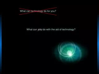
What can technology do for you?. What can you do with the aid of technology?. Use technology to gain insights into the processes of nature… How? Examine controlled physical interactions between matter and energy microscopy spectroscopy. Why look at surfaces at high magnification?

E N D
What can technology do for you? What can you do with the aid of technology?
Use technology to gain insights into the processes of nature… How? Examine controlled physical interactions between matter and energy microscopy spectroscopy Why look at surfaces at high magnification? Description and identification of constituent phases by morphology, emission and absorption properties, or other physical responses. Observation of features which give you insight into processes and the relevant mechanisms. What is chemical microanalysis all about and why do it? Phase identification by element ID and stoichiometry. Identify and quantify chemical processes. Establish qualitatively and quantitatively the distribution of elements in a sample at the micro-scale, and quantify kinetic processes. Provide quantitative data for thermodynamically constrained processes (establish the temperature, pressure, solution activities, etc. of chemical reactions in nature.)
Resources and engineering Planetary processes
The array of microanalysis tools…sorting through the acronyms XAFS SCEM MFM LA-ICP-MS STM PIXE XANES LRS SEM-EDS TAP FIM SHRIMP SPM μ-XRD SIMS IRAS LEED ESCA LEIS EPMA UV-VIS STEM ARPES LEXES FTIR μ-XRF nanoSIMS TEM PEEM CFM AES EBSD EELS HIM HAS XPS AFM
The array of microanalysis tools… Electron excitation and absorption techniques SEM – Scanning electron microscopy EPMA – Electron probe microanalysis LEXES – low energy electron induced x-ray emission spectroscopy TEM-STEM – Transmission electron microscopy (and scanning transmission electron microscopy or “analytical electron microscopy” = AEM) EELS – electron energy loss spectroscopy EBSD – electron backscatter diffraction in SEM AES – Auger electron spectroscopy Photon excitation and absorption techniques Optical Microscopy XPS – X-ray photoelectron microscopy (or ESCA = electron spectroscopy for chemical analysis) FTIR – fourier transform infrared analysis UV-VIS Laser Raman Spectroscopy μ-XRF – micro-X-ray fluorescence X-ray microdiffraction Synchrotron techniques XANES XAFS Photon ablation LA-ICP-MS – Laser ablation inductively coupled plasma mass spectrometry Ion ablation and activation (focused ion beam techniques) SIMS-Ion Microprobe – Secondary ion mass spectrometry SHRIMP – sensitive high resolution ion microprobe nanoSIMS He-ion microscopy Other SPM – Scanning probe microscopies STM – Scanning tunneling microscopy AFM – Atomic force microscopy MFM – Magnetic force microscopy Atom probe (TAP) tomographic atom probe or atom probe microscopy (APM) LA-WATAP (laser assisted wide angle) PIXE – proton induced x-ray emission
The array of microanalysis tools… Electron excitation and absorption techniques SEM – Scanning electron microscopy EPMA – Electron probe microanalysis LEXES – low energy electron induced x-ray emission spectroscopy TEM-STEM – Transmission electron microscopy (and scanning transmission electron microscopy or “analytical electron microscopy” = AEM) EELS – electron energy loss spectroscopy EBSD – electron backscatter diffraction in SEM AES – Auger electron spectroscopy Photon excitation and absorption techniques Optical Microscopy XPS – X-ray photoelectron microscopy (or ESCA = electron spectroscopy for chemical analysis) FTIR – fourier transform infrared analysis UV-VIS Laser Raman Spectroscopy μ-XRF – micro-X-ray fluorescence X-ray microdiffraction Synchrotron techniques XANES XAFS Surface imaging down to a few Å (or less) – primarily morphology Quantitative microanalysis and compositional imaging Ultra low kV X-ray microanalysis (10’s of μm) at low voltage Imaging by electron transmission for extreme magnification of internal structure. Compositional analysis, bonding and valence (low Z) Microstructural analysis Ultra low energy surface analysis for elemental composition Similar to XPS, but higher spatial resolution (10-100nm) Microstructural observation, including polarization properties Surface (upper few nm) chemical analysis (parts per thousand) Spatial resolution 100’s of μm Molecular fingerprinting Analysis of transition metal ions, organic compounds Vibrational modes – molecular identification via bond info. Quantitative analysis of major and minor elements, 100s of μm Microstructural analysis Valence and coordination, material band structure Scattering of photoelectrons from surrounding atoms = local structure.
The array of microanalysis tools… Photon ablation LA-ICP-MS – Laser ablation inductively coupled plasma mass spectrometry Ion ablation and activation (focused ion beam techniques) SIMS-Ion Microprobe – Secondary ion mass spectrometry SHRIMP – sensitive high resolution ion microprobe nanoSIMS He-ionmicroscopy (HIM) Other SPM – Scanning probe microscopies STM – Scanning tunneling microscopy AFM – Atomic force microscopy MFM – Magnetic force microscopy Atom probe (TAP) tomographic atom probe or atom probe microscopy (APM) LA-WATAP (laser assisted wide angle) PIXE – proton induced x-ray emission Trace elements and isotopic compositions, 10’s to 100’s of microns (ppt in some cases), destructive. Ion mass/charge ratios, 10-30 microns, ppm-ppb sensitivity, isotope ratios and geochronology (destructive) Isotope ratios (limited range, 10’s of nanometers) Ultra high resolution surface imaging – RBS possible Surface atomic imaging (conductors) – nm or less, indirect Surface atomic imaging – 0.1nm – direct Surface magnetic structure Atom scale 3D composition (destructive) TAP on insulators Compositional analysis down to μm scale (accelerator)
Surface imaging SEM STM - atomic AFM - atomic EBSD - SEM AES XPS SIMS Surface chemistry SIMS AES XPS TAP-APM EPMA – LEXES (WDS) Chemical analysis of microvolumes Elemental concentrations SEM - EDS EPMA (WDS) LA-ICP-MS μ-XRF SIMS PIXE FTIR (bonding, functional groups) Chemical analysis of microvolumes Isotopic concentrations LA-ICP-MS SIMS Analysis of microstructure TEM-STEM EBSD - SEM X-ray microdiffraction STM AFM TAP-APM
Micro-scale SEM - EDS EPMA SIMS (ablation) AES (surface) XPS (surface) Nano-scale HR-SEM-EDS He-ion microscope EPMA (special) TEM-STEM-EDS STM (atomic scale) AFM (atomic scale) NanoSIMS (ablation) TAP-APM (atomic scale)
Electron… Elementary particle (no internal structure) Fermion (Half integer spin, constrained by Pauli Exclusion principle) Lepton (do not interact through the color force = no strong interaction) of charge -1, mass = 0.511 MeV/c2 Electron properties and interaction with matter Wavelength (0.01-0.04nm) much shorter than visible light (400-650nm) Charged, so will interact with EM fields – can be focused Interact with matter Elastically -Backscatter Inelastically – to produce Secondary electrons light X-rays heat (phonon excitation/lattice oscillation)
Data? Observations… Size, shape, relationships of objects (What does what you “see” actually represent?) Paleotemperature, pressure, solution activities, age, etc. Calculated results with assumptions… Elemental concentration…do we actually measure this? Measured… Intensities of X-rays at specified wavelengths Mass ratios
Scanning Electron Microscopy and Electron Microprobe Analysis • Non-destructive • In-situ analysis • High magnification surface imaging • Chemical analysis of materials on a scale of microns (or less) • Focused electron beam generates detectable signals from specimen • Secondary electrons • Backscattered electrons • X-rays
Scanning Electron Microscope Focused electron beam is scanned over surface - excites atoms of target – signals emitted and detected High magnification surface imaging with resolution of few nm to sub-nm for secondary electrons
Scanning Electron Microscope Artificial artery V-oxide Zeolite surface foraminifera
Electron Microprobe (Electron Probe Microanalysis - EPMA) quantitative chemical microanalysis and compositional imaging Primarily designed for precise characteristic X-ray detection X-ray wavelengths relate to electronic structure – can identify specific elements. Intensity variation in specimen relates to spatial distribution of these elements X-ray counts from specimen compared to standards of known composition → computed elemental concentrations
PURPOSE • Analysis of individual mineral grains or amorphous solid phases • In-situ (preserve textural relationships!) • Compositional imaging and spatial distribution of elements in the scanned area. • Quantitative chemical variation within mineral grains or discrete phases - zoning and growth histories Mg Kα
Ag distribution in solder Solder bumps on IC 50 μm Y distribution in natural monazite
GENERAL “LIMITATIONS” • Spatial resolution – it depends Electron beam focused to 0.01 to 0.2 μm diameter Scattering → electron interaction volume and signal emission volume. Imaging (SEM) – from few nm to hundreds of nm Chemical analysis (EPMA) - Silicates 1 to 3 μm diameter volume • Compositional sensitivity (detection limits) – it depends 50-200 ppm (a few ppm in some special cases) • For EPMA, mostly major and minor elements Element range Routinely Na and heavier – but it depends… Also B, C, N, O (special circumstances)
ELECTRONS λ shorter than visible light → higher image resolution (light 400-650nm, electrons ~ 0.04 -.01nm,1-10kV) Charged particles - can be electromagnetically focused Interact with specimen to produce detectable signals BSE SE X-Rays
ELECTRON OPTICS • Electron source (gun) Cathode + Anode Controls beam voltage • Condenser lenses Controls beam current • Objective lens Controls beam size, shape, depth of field at specimen Result = electron beam of specified voltage, current and diameter. Wavelength dispersive, X-ray spectrometer Vacuum System - mean path length of electrons must be greater than column length 10-3 to 10-5 pa (~10-5 to 10-7torr) specimen
What happens when beam reaches specimen? • Beam/Specimen interactions • Some beam electrons scattered back out • -More effectively by heavier target atoms • -Results in BSE signal • 2) Some beam electrons interact inelastically with atoms in the target • Energy is transferred • A) Can result in ejection of some weakly bound outer shell electrons → secondary electron signal (low energy) • B) Some cause inner shell ionizations leading to characteristic X-ray emission 15 kV 1 mm 10 kV Electron trajectory modeling - Casino Labradorite (Z = 11)
INNER SHELL IONIZATION • If energy equal or greater than critical excitation potential… • Can eject inner shell electron • 2) Atom wants to return to ground state • outer shell electron fills vacancy – relaxation • Outer shell electron in higher energy state relative to inner shell electron • some energy surplus in the transition • → photon emission (X-ray) X-ray is characteristic of the target element Example: E SiKα = 1.740 KeV (7.125Å) E FeKα = 6.404 KeV (1.936Å)
ψp1 ψp Kα ψp2 ψ1s
ψp1 ψp Kβ ψp2 ψ1s
Also produce background spectrum Originates from deceleration reactions of insufficient energy to ionize the target atom Produce overall X-ray spectrum Characteristic peaks superimposed on a background
How are X-rays detected? Discriminated by energy (EDS) Or wavelength (WDS) EDS Detectors Solid state semiconductor detectors See entire spectrum at once Fast Relatively low resolution crystal WDS Select analytical lines by diffraction nλ = 2d sin θ Relatively high resolution WDS used for most quantitative analysis EDS for qualitative evaluation sample detector (counter)
Wavelength Dispersive Spectrometry (WDS) Bragg Law: nλ = 2d sinθ θ d At certain θ, rays will be in phase, otherwise out of phase = destructive interference
Detectors • Usually gas filled counter tubes • ionize counter gas (Xe, Ar) • eject photoelectron • photoelectron ionizes other gas atoms • electrons collected by wire • output pulse = x-ray count • pulse height proportional to x-ray energy
Measure counts per second of a particular X-ray compare to standard of known composition to get concentration Must correct for matrix effects Z atomic # A absorption Fsecondary fluorescence
IMAGING Incident beam Object: Convert radiation into an electrical signal which is then amplified Select Secondary electrons Backscattered electrons X-rays Auger electrons Photons from Cathodoluminescence Absorbed electron current Light (cathodoluminescence) Auger electrons Secondary electrons Bremsstrahlung Characteristic X-rays Backscattered electrons Sample heat Any of the collected signals can be displayed as an image if you either scan the beam or the specimen stage Elastically scattered electrons Specimen current Transmitted electrons Secondary electron detector electron strikes scintillator and converted to light pulse - Amplified and displayed Raster the beam over sample and display at the same time and get image (basically an intensity map) Scan smaller and smaller areas to increase magnification 5 mm
Electron Backscatter Backscattering more efficient with heavier elements Can get qualitative estimate of average atomic number of target Image will reveal different phases Brighter = higher average Z
X-ray mapping display spatial distribution of characteristic X-ray intensity to get qualitative compositional information Garnet, Grand Canyon MgKα Garnet - Moretown Formation, MA CaKα Garnet - Italy MgKα Garnet – Grand Canyon MnKα
plag opx matrix plag Cpx + qtz garnet opx+plag+ mt Original opx Corona texture - CaKα Saskatchewan
calcite 100 μm Monazite – thorium map Lobster cuticle – composite element map
Quantitative Analysis – Geosciences applications • Mineral chemistry – in-situ, single phase characterization microscale compositional changes within phases - zoning • Crystallization paths and evolution of magmatic systems • Geothermometry • Geobarometry • Geochronology • Low-temperature geochemistry clay mineralogy mass transfer / weathering reactions paleoclimate applications – speleothem microchemistry • Fundamental geochemical processes Phase equilibria Kinetics distribution coefficients
Two generations of garnet growth Black Hills, SD grossular spessartine
Cladding Core Cladding Element concentrations in optical fiber
ThMα Geochronology – traditionally using isotopic/mass-spectrometric techniques • IDTIMS • Ion Probe Electron Microprobe (EPMA) • High spatial resolution access to ultra-thin rims, micro-domains, and inclusions • In-situ: relate composition (and age) to micro/macro-structure and mineral paragenesis • Non-destructive • Integrated spatial / compositional / age relationships Monazite: LREE-phosphate with Th and U (→ radiogenic Pb) Common accessory phase in many rocks Fabric former Dissolution/re-precipitation reactions result in polygenetic nature, and ties into overall reaction history Dating events{
Map compositional domains, then quantitatively measure Th, U, and Pb concentrations. Compute age via:
CeB6 /LaB6 New HV power supply Decouple operation of condensers to optimize brightness down column Current regulation up to 1 microamp The Ultrachron Project Electron optics • Optimize analytical resolution (Smaller phase analysis) for a range of kV and current • High, stable current for trace element analysis • Minimize excitation volume in high Z material Detection BSE and X-Ray optics • Improve precision (Optimize counting - PbMα) • Integrate spectrometers • Improve accuracy – background estimation Techniques • Minimize beam damage • Background • Analytical protocols Improve dynamic range of BSE amplifier BSE shielding for high current applications New high intensity crystals (VLPET) + VL detectors Counters optimized (gas mixture, pressure, HV) Completely dry vacuum system Anticontamination
ψp ψp ψp ψ1s