Xilinx Virtex-5 FPGA Clocking
80 likes | 563 Vues
Xilinx Virtex-5 FPGA Clocking. Presented by: Wesley Holland. Global Clock Lines. Each Virtex-5 device has 32 global clock lines (GCLs) for clocking sequential resources GCLs are available anywhere on chip

Xilinx Virtex-5 FPGA Clocking
E N D
Presentation Transcript
Xilinx Virtex-5 FPGA Clocking Presented by: Wesley Holland
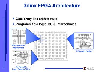
Global Clock Lines • Each Virtex-5 device has 32 global clock lines (GCLs) for clocking sequential resources • GCLs are available anywhere on chip • GCLs are designed to have low skew, low duty cycle distortion, low power, improved jitter tolerance, and to support very high frequency signals • GCLs are differential for noise rejection • Tree topology, with unused branches disconnected • GCLs can be driven by the following sources: • Global clock inputs (pins – can also double as GP I/O) • Other GCLs • General logic interconnect • Clock Management Tiles (CMTs)
Regional Clock Lines • Regional clock lines are independent of the global clock network • These clock trees are also designed for low-skew and low-power operation • Unused branches are disconnected • A regional clock is accessible only within a clock region and that region’s neighbors
Clock Management Tiles (CMTs) • CMTs provide flexible, high-performance clocking • Each CMT contains two digital clock managers (DCMs) and one PLL • DCMs provide following features: • Clock deskewing via contained DLL • Frequency synthesis by integer multiplication and division • Phase shifting • Dynamic reconfiguration • The main functions of the PLL are: • Clock network deskewing • Standalone frequency synthesis • Jitter filtering
Conclusions • Deskewing methods: deskew buffers (in DCMs) • Power considerations: conditional clocks • Maximum clock rate: 550 MHz • Maximum skew: 480 ps for XC5VLX110T (mid-range device) • Maximum skew percentage: 26.4% • Clock distribution topology: tree • CMT features: • Clock deskewing • Frequency synthesis • Phase shifting • Dynamic reconfiguration • Jitter filtering
References • http://direct.xilinx.com/bvdocs/userguides/ug190.pdf • http://direct.xilinx.com/bvdocs/publications/ds202.pdf