Xilinx FPGA Architecture
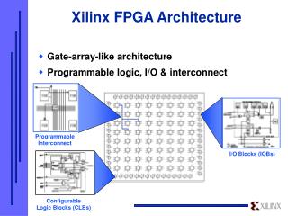
Xilinx FPGA Architecture. Gate-array-like architecture Programmable logic, I/O & interconnect. Programmable Interconnect. I/O Blocks (IOBs). Configurable Logic Blocks (CLBs). Logic Cell Capacity. A better first-order alternative to gate counting Better comparisons among different FPGAs

Xilinx FPGA Architecture
E N D
Presentation Transcript
Xilinx FPGA Architecture • Gate-array-like architecture • Programmable logic, I/O & interconnect Programmable Interconnect I/O Blocks (IOBs) Configurable Logic Blocks (CLBs)
Logic Cell Capacity • A better first-order alternative to gate counting • Better comparisons among different FPGAs • Logic cell definition: • 4-input look-up table + dedicated flip-flop • Logic cells per CLB: • XC4000 2.375 (2 4-LUTs, 1 3-LUT, 2 FFs) • Spartan 2.375 (2 4-LUTs, 1 3-LUT, 2 FFs) • Virtex 4.5 (4 4-LUTs, 1 F5MUX, 4 FFs) • XC5200 4 (4 4-LUTs, 4 FFs)
Configurable Logic Block (CLB) • Combinational logic generated in a lookup table (LUT) • Any function of available inputs • LUT output feeds CLB output or D input of flip-flop Combinational Logic Function (LUT) Flip- Flop Outputs Inputs
XC4000/Spartan Series Function Generators • Two 4-input function generators • Independent inputs (2 functions of 4 inputs) • One 3-input function generator • Independent inputs • Combines 4-input functions to make any 5-input function & some 9-input functions F H G
Lookup Table • Generates any function of its inputs • Typically 4 inputs • Logically equivalent to a 16x1 ROM InputsOutput 0000 0 0001 1 0010 1 0011 0 LUT
Targetting LUT-based Logic • LUT limit is on inputs, not complexity • Reducing inputs/function (fan-in) to fit CLBs improves density and speed • Automatically done by Xilinx synthesis and implementation tools • Inverters are free CLB Lookup Table
Duplicating Logic Can Improve Results • Collapsing of logic into CLBs affects number of levels required and therefore speed • The gates you use will determine mapping • Nets with a fanout >1 may be outside a CLB O1 O1 I1 N1A I1 N1 N1B N1 must go to two places, so O1 may require a second level of logic Duplicating first gate allows N1A to always be collapsed inside a single lookup table
Defining Lookup Tables with Gate Primitives • Example of gate primitive • Up to five inputs with all combinations of inversion • AND2B1 indicates 1 “bubbled” or inverted input • Up to nine inputs non-inverted • Add external INV primitives if desired AND2
Flip-Flops • Stores data (D) on rising edge of clock (K) • Clock Enable (CE) • Asynchronous Clear (C) K CE C D Q X X 1 X 0 1 0 D D 0 X 0 X Q D Q CE K C
Additional Flip-Flop Controls • Reset (Clear) or Set • Global initialization (GSR) • Programmable clock polarity • Clock enable can be left unconnected
Use Global Reset • All flip-flops initialized on configuration and global net • Source of global net specified via STARTUP component Q2 GSR Q3 GTS STARTUP Q1Q4 DoneIn CLK
Direct Input • Direct Input bypasses LUT and goes directly to flip-flop • Provides higher speed if no logic is required • Frees LUT for other functions DIN D Q LUT
On-Chip RAM • All Xilinx FPGAs use RAM-based programming • Adding Write Enable to LUT creates on-chip SelectRAM memory
Data Write Enable Output Address Data Write Enable Output Write Clock Address Data Write Enable Single-Port Output Write Clock Write Address/ Single-Port Read Address Dual-Port Output Dual-Port Read Address SelectRAM Benefits • Asynchronous • Compatible with original XC4000 • Synchronous • Simpler timing • Dual-Port
Write Clock • Same clock as for flip-flops • Programmable polarity • Independent of flip-flop polarity • Self-timed write • Latches data, write enable, address on edge • Generates write pulse • No effect on read operation
Supported RAM Modes • Per CLB: 16 x 1 16 x 2 32 x 1 Edge- Triggered Timing Level- Sensitive Timing Single- Port X X X X X Dual- Port X X
I/O Block (IOB) • Periphery of identical I/O blocks • Input, output, or bidirectional • Direct or registered (or latched input) • Pullup/pulldown • Programmable slew rate • Three-state output • Programmable thresholds IOB I Pad O TS Bonded to Package Pin Clocks
IPAD IBUF Use Special IOB Primitives • User explicitly defines what resources in the IOB are to be used • I/Os are defined with • 1 pad primitive • At least 1 function primitive • 1 input element, 1 output element or both • Inverters may also be pulled into IOBs
Locking Down I/O Locations • LOC=Pxx attribute defines I/O pad location(s) • Avoid locking IOBs early • Makes routing more difficult • Use IOB LOC= to lock pins late in design cycle once PCB is built • Can lock IOBs if floorplanning the connected CLBs
IPAD IBUF Use Pullups/Pulldowns • Pullup automatically connected on unused IOBs • User can specify PULLUP or PULLDOWN primitive on used IOBs • Inputs should not be left floating • Add pullup to design inputs that may be left floating to reduce power and noise
External Clock Routed Clock X External Data X Delay Data Faster Setup with NODELAY • Delay included by default • Compensates for clock routing delay to prevent hold time • NODELAY attribute removes delay element • Creates hold time Example IOB External Data Pad Q D Delay Input Buffer External Clock Routing Delay Pad
FAST OPAD OBUF Slew Rate Control • Slew rate controls output speed • Default slow slew rate reduces noise & ground bounce • Use fast slew rate wherever speed is important • FAST parameter on output logic primitive
OBUFE OE T Output Three-State Control • Free inverter on output buffer control • Use OBUFE macro for active-high enable • Use OBUFT primitive for active-low enable OBUFT OE T
Global Three-State • 3-state control either local and/or via a dedicated global net • Global three-state controlled by STARTUP primitive STARTUP GTS GSR
I/O Thresholds • 5V devices have globally selectable TTL or CMOS I/O thresholds • Inputs and outputs separately controllable • Default is TTL • 3V devices can interface to 5V or 3V logic • 2.5V Virtex devices have programmable interfaces
Programmable Interconnect • Resources to create arbitrary interconnection networks • Various types of interconnect • Flexible general-purpose interconnect • Low-skew long lines • Internal three-state buffers Long Lines CLB CLB Switch Matrix General Purpose CLB CLB
Interconnect • Single-length, double-length, and long lines • Clock buffers and dedicated long lines • Global set/reset and global three-state
Fast Direct Interconnect • Direct connections from CLB to adjacent CLB or IOB • Fastest interconnect • < 1 ns delay • Carry logic uses direct interconnect
Flexible General-Purpose Interconnect • Flexible but slow if crosses many channels • Programmable switch matrix at each channel crossing • Connects across, changes direction or fans out • Single-Length lines • Double-Length lines skip every other switch matrix
Switch Matrix • Bidirectional pass transistors • High routing flexibility
Reduce Fanout • Higher fanout nets (>16 loads) are harder to route & slower • Consider duplicating source in schematic to improve routing or speed fn1 fn1 D Q D Q fn1 D Q
Long Lines for High Fanout Nets • Metal lines that traverse length & width of chip • Lowest skew • Ideal for high fan-out signals • Ideal for clocking • Requires vertical or horizontal alignment of loads CLB CLB CLB CLB
Advantages of Vertical Orientation • Bidirectional data bus lines run horizontally • Enable lines run vertically • Large registered functions align vertically • Clock lines run vertically • Most non-clock, non-BUFT long lines run vertically • Carry logic runs vertically D Q D Q D Q D Q D Q D Q D Q D Q
Use Global Clock Buffers • Use clock buffers for highest fanout clocks • Drive high-speed long line resources • <2ns skew across a device • No internal hold times • Use generic BUFG primitive • Allows software to choose best type of buffer • Allows easy migration across families
D IPAD BUFG Using a Clock Generated Off-Chip • Connect IPAD directly to clock buffer primitive • Required for BUFGP • Place & route uses special fast input pin • Provides higher speed and uses fewer routing resources
Internal Oscillator • Oscillator used to generate configuration clock can be used after configuration as part of design • +/- 50% frequency range • Can be divided down to desired frequency range
Use BUFT for Buses • BUFT references internal three-state buffers • Use to multiplex signals onto long routing lines to use as buses • Multiplexer macros use lookup tables (M4_1E, etc.) _ENABLE_A _ENABLE_B A3 B3 BUS<3> A2 B2 BUFT BUS<2> A1 B1 BUS<1> A0 B0 BUS<0>
BUFT Output Net Never Floats • Cross-coupled inverters remember last value to insure that line never floats • Valid signal is always read from output of BUFT • No need to reference “keeper” circuit
Special Resources • Arithmetic/counter carry logic • Wide decode or cascade functions • Configuration • Boundary scan (JTAG)
Carry Logic • Use carry logic in CLBs to increase arithmetic speed • High density via serial implementation of carry • Carry propagates in upward direction • Use library’s carry-based macros (RPMs) or LogiBLOX synthesis carry CLB carry CLB carry CLB
Wide Decoders • Decoder is effectively a dedicated wired-AND • 4 decoder lines per edge • Direct inputs from all IOBs on an edge • Half as many general inputs • Useful for address decoding
Using Wide Decoders • Use DECODEx macro • Diamond indicates open-drain • Can tie multiple outputs together • Must use a PULLUP primitive DECODE8 A0 A1 A2 A3 A4 A5 A6 A7 O
Use WANDx symbol (Horizontal Long Line) BUFT BUFT BUFT A B H Wide Wired-AND Using Three-State Buffers WAND8 I1 I2 I3 I4 I5 I6 I7 I8 O Underlying implementation
Configuration • Schematic or HDL description is converted to a configuration file by the Xilinx development system • Configuration file is loaded into FPGA on power-up • Stored in configuration latches • Controls CLBs, IOBs, interconnect, etc.
Configuration Bitstream • Binary programming file • Length depends only on device, not utilization • Typically 1 ms per bit (total from a few ms to <1s) • FPGA can load its configuration automatically on power-up, or under microprocessor control • Can be loaded directly into device/configuration PROM
Configuration Modes • Bit-serial configuration • Simple, uses few device pins • Controlled by FPGA (Master) or externally (Slave) • Xilinx Serial PROMs available • Byte-parallel configuration • Can drive PROM addresses (Master) • Can be microprocessor-controlled (Peripheral)
Configuration Pins • Configuration starts on power-up • Mode pin(s) checked to determine method • Usable as extra I/O after configuration • All I/O not used for configuration are disabled • Reconfiguration possible by pulling PROGRAM pin Low • No partial configuration
READBACK CLK DATA TRIG RIP Readback • Configuration data can be read back serially • Allows verification of programming • Readback data can include user-register values • Allows in-circuit functional verification • Requires READBACK symbol
Boundary Scan • IEEE 1149.1-compatible boundary scan (JTAG) • Available before configuration • Configuration & readback possible via boundary scan logic
Power Consumption • CMOS SRAM technology provides low standby power • Operating power is mostly dynamic • Proportional to transition frequency of internal nodes • Xilinx segmented interconnect minimizes amount of metal capacitance to switch, minimizing power