Download

1 / 39
570 likes | 1.28k Vues
FPGA Architecture. Presentation Overview. Available choice for digital designer FPGA – A detailed look Interconnection Framework FPGAs and CPLDs Field programmability and programming technologies SRAM, Anti-fuse, EPROM and EEPROM Design steps Commercially available devices Xilinx XC4000

E N D
Presentation Overview • Available choice for digital designer • FPGA – A detailed look • Interconnection Framework • FPGAs and CPLDs • Field programmability and programming technologies • SRAM, Anti-fuse, EPROM and EEPROM • Design steps • Commercially available devices • Xilinx XC4000 • Altera MAX 5000
Designer’s Choice • Digital designer has various options • SSI (small scale integrated circuits) or MSI (medium scale integrated circuits) components • Difficulties arises as design size increases • Interconnections grow with complexity resulting in a prolonged testing phase • Simple programmable logic devices • PALs (programmable array logic) • PLAs (programmable logic array) • Architecture not scalable; Power consumption and delays play an important role in extending the architecture to complex designs • Implementation of larger designs leads to same difficulty as that of discrete components
Designer’s Choice • Quest for high capacity; Two choices available • MPGA (Masked Programmable Logic Devices) • Customized during fabrication • Low volume expensive • Prolonged time-to-market and high financial risk • FPGA (Field Programmable Logic Devices) • Customized by end user • Implements multi-level logic function • Fast time to market and low risk
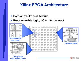
FPGA – A Quick Look • Two dimensional array of customizable logic block placed in an interconnect array • Like PLDs programmable at users site • Like MPGAs, implements thousands of gates of logic in a single device • Employs logic and interconnect structure capable of implementing multi-level logic • Scalable in proportion with logic removing many of the size limitations of PLD derived two level architecture • FPGAs offer the benefit of both MPGAs and PLDs!
FPGA – A Detailed Look • Based on the principle of functional completeness • FPGA: Functionally complete elements (Logic Blocks) placed in an interconnect framework • Interconnection framework comprises of wire segments and switches; Provide a means to interconnect logic blocks • Circuits are partitioned to logic block size, mapped and routed
A Fictitious FPGA Architecture(With Multiplexer As Functionally Complete Cell) • Basic building block
Interconnection Framework • Granularity and interconnection structure has caused a split in the industry • FPGA • Fine grained • Variable length interconnect segments • Timing in general is not predictable; Timing extracted after placement and route
Interconnection Framework • CPLD • Coarse grained (SPLD like blocks) • Programmable crossbar interconnect structure • Interconnect structure uses continuous metal lines • The switch matrix may or may not be fully populated • Timing predictable if fully populated • Architecture does not scale well
Field Programmability • Field programmability is achieved through switches (Transistors controlled by memory elements or fuses) • Switches control the following aspects • Interconnection among wire segments • Configuration of logic blocks • Distributed memory elements controlling the switches and configuration of logic blocks are together called “Configuration Memory”
Technology of Programmable Elements • Vary from vendor to vendor. All share the common property: Configurable in one of the two positions – ‘ON’ or ‘OFF’ • Can be classified into three categories: • SRAM based • Fuse based • EPROM/EEPROM/Flash based • Desired properties: • Minimum area consumption • Low on resistance; High off resistance • Low parasitic capacitance to the attached wire • Reliability in volume production
SRAM Programming Technology • Employs SRAM (Static RAM) cells to control pass transistors and/or transmission gates • SRAM cells control the configuration of logic block as well • Volatile • Needs an external storage • Needs a power-on configuration mechanism • In-circuit re-programmable • Lesser configuration time • Occupies relatively larger area
Anti-fuse Programming Technology • Though implementation differ, all anti-fuse programming elements share common property • Uses materials which normally resides in high impedance state • But can be fused irreversibly into low impedance state by applying high voltage
Anti-fuse Programming Technology • Very low ON Resistance (Faster implementation of circuits) • Limited size of anti-fuse elements; Interconnects occupy relatively lesser area • Offset : Larger transistors needed for programming • One Time Programmable • Cannot be re-programmed • (Design changes are not possible) • Retain configuration after power off
EPROM, EEPROM or Flash Based Programming Technology • EPROM Programming Technology • Two gates: Floating and Select • Normal mode: • No charge on floating gate • Transistor behaves as normal n-channel transistor • Floating gate charged by applying high voltage • Threshold of transistor (as seen by gate) increases • Transistor turned off permanently • Re-programmable by exposing to UV radiation
EPROM Programming Technology • Used as pull-down devices • Consumes static power
EPROM Programming Technology • No external storage mechanism • Re-programmable (Not all!) • Not in-system re-programmable • Re-programming is a time consuming task
EEPROM Programming Technology • Two gates: Floating and Select • Functionally equivalent to EPROM; Construction and structure differ • Electrically Erasable: Re-programmable by applying high voltage (No UV radiation expose!) • When un-programmed, the threshold (as seen by select gate) is negative!
EEPROM Programming Technology • Re-programmable; In general, in-system re-programmable • Re-programming consumes lesser time compared to EPROM technology • Multiple voltage sources may be required • Area occupied is twice that of EPROM!
An Example • Modulo-4 counter: Logic Implementation • Modulo-4 counter: Specification
Design Steps Involved in Designing With FPGAs • Understand and define design requirements • Design description • Behavioural simulation (Source code interpretation) • Synthesis • Functional or Gate level simulation • Implementation • Fitting • Place and Route • Timing or Post layout simulation • Programming, Test and Debug
Commercially Available Devices • Architecture differs from vendor to vendor • Characterized by • Structure and content of logic block • Structure and content of routing resources • To examine, look at some of available devices • FPGA: Xilinx (XC4000) • CPLD: Altera (MAX 5K)
Xilinx FPGAs • Generic Xilinx Architecture • Symmetric Array based; Array consists of CLBs with LUTs and D-Flipflops • N-input LUTs can implement any n-input boolean function • Array embedded within the periphery of IO blocks • Array elements interleaved with routing resources (wire segments, switch matrix and single connection points) • Employs SRAM technology
XC 4000 • 3 LUTs and 2 Flip-flops in a two stage arrangement • 2 Outputs: Can be registered or combinational • External signals can also be registered • More of internal signals are available for connections • Can implement any two independent functions of four variables or any single function of five variables • XC4000 CLB
XC4000 • XC4000 Routing Architecture
XC 4000 • XC4000 Routing Architecture • Wire segments • Single length lines • Spans single CLB • Connects adjacent CLBs • Used to connect signals that do not have critical timing requirements • Double length lines • Spans two CLBs • Uses half as much switch as a single length connection • Long lines • Low skew; Used for signals such as clock • Relatively rare resource • Switch Matrix • Every line is connected to lines on the other three direction • Each connection requires six transistors
ALTERA CPLDS • Altera generic architecture • Hierarchical PLD structure • First level: LABs (Functional blocks); LAB is similar to SPLDs • Second Level: Interconnections among LABs • LAB consists of • Product term array • Product term distribution • Macro-cells • Expander product terms • Interconnection region: PIA • EPROM/EEPROM based • Example: MAX5K, MAX7K
MAX 5000 • MAX5K Macrocell • Three wide AND gate feed an OR gate (Sum of products) • XOR gate may be used in arithmetic operations or in polarity selection • One flipflop per macrocell; Outputs may be registered • Flipflop preset and clear are via product terms; Clock may be either system clock or internally generated • Output may be driven out or fedback • Feedback is both local and global; Local feedback is within macrocell and is quicker
MAX 5000 • MAX5000 Expander Product Term • Number of product terms to macrocell limited • Wider functions implemented via expander product terms • Foldback NAND structure • Inputs are from PIA, expander product term and macrocell feedback • Outputs of expander product term are sent to other macrocell and to itself
MAX 5000 • MAX5000 Architecture • Second level of hierarchy: connections among LABs • LABs are connected via PIA • Interconnections may be global or local; Global interconnects uses PIA • PIA consists of long wiring segments: • Spans entire length of chip and passes adjacent to each LAB • PIA fully populated • Predictable timing
SRAM FPGA -- EEPROM FPGA • An FPGA is similar to several other types of devices which have been around for quite a while, the difference being that an FPGA is simply much more expandable and versatile. The devices which FPGAs get compared to most often are CPLDs (Complex Programmable Logic Devices), which are similar in function but typically have way less logic gates inside them; Customizable CPU design is much more feasible with an FPGA. Once upon a time, CPLDs also had the distinct advantage of retaining their configuration even
SRAM FPGA -- EEPROM FPGA • when turned off; When FPGAs first came out, they used simple SRAM to hold their configuration, which of course would be lost when the device lost power. Back then, the FPGA had to be programmed from scratch every time it was turned on, usually from a separate serial ROM chip. But today, FPGAs come in Flash, EPROM, and EEPROM variants, which will retain configuration, and which can also be re-programmed. (Fuse and anti-fuse FPGAs also exist, which act like PROMs in that they are one-time programmable, and cannot be reprogrammed
SRAM FPGA -- EEPROM FPGA • afterward.) Despite this, however, most FPGAs still use SRAM for reasons of simplicity (when you need to reprogram it, it's easier to re-encode a small ROM chip than to reprogram a large FPGA chip), so count on having to use a separate boot ROM for the FPGA. • Use of an FPGA is broadly divided into two main stages: The first is "configuration mode", the mode in which the FPGA is when you first power it up. Configuration mode is, as you may have guessed, where you configure the FPGA; That is,
SRAM FPGA -- EEPROM FPGA • this is when you load your code into it, dictating how the pins behave. Once configuration is complete, the FPGA goes into "user mode", its main mode of operation, where the programmed circuit actually starts functioning.
Product – FPGA vs ASIC Comparison: • FPGA benefits vs ASICs:- Design time: 9 month design cycle vs 2-3 years- Cost: No $3-5 M upfront (NRE) design cost. No $100-500K mask-set cost- Volume: High initial ASIC cost recovered only in very high volume products • Due to Moore’s law, many ASIC market requirements now met by FPGAs- Eg. Virtex II Pro has 4 processors, 10 Mb memory, IO Resulting Market Shift: • Dramatic decline in number of ASIC design starts:- 11,000 in ’97 - 1,500 in ’02 • FPGAs as a % of Logic market:- Increase from 10 to 22% in past 3-4 years • FPGAs (or programmable logic) is the fastest growing segment of the semiconductor industry!!
FPGA Cost Advantage FPGA Cost Advantage FPGA Cost Advantage ASIC Cost Advantage ASIC Cost Advantage FPGA/ASIC Crossover Changes 90nm / 300mm ASICs Cost 150nm / 200mm ASICs 90nm / 300mm FPGAs 150nm / 200mm FPGAs Production Volume