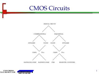
CMOS Digital Integrated Circuits
CMOS Digital Integrated Circuits. Lec 3 MOS Transistor I. Goals Understand the basic MOSFET operation Learn the components of the threshold voltages Be able to handle body effect Be able to calculate drain currents for MOSFET Be able to extract basic MOSFET static parameters from I-V plots.

CMOS Digital Integrated Circuits
E N D
Presentation Transcript
CMOS Digital Integrated Circuits Lec 3 MOS Transistor I
Goals • Understand the basic MOSFET operation • Learn the components of the threshold voltages • Be able to handle body effect • Be able to calculate drain currents for MOSFET • Be able to extract basic MOSFET static parameters from I-V plots
VG A D I VB MOS Transistor BasicsTwo Terminal Structure Two terminal structure (p-substrate): The MOS capacitor • Important derived parameters. With VG = VB = 0: • F – Buck Fermi Potential (Substrate) • S – Surface Potential (Substrate)
MOS Transistor BasicsTwo Terminal Structure (Continued) • VFB– Flat Band Voltage (applied external voltage to G-B to flatten bandsof substrate – equal to built-in potential difference of MOS – equal to work function difference GBbetween the substrate (channel) and gate. • Operation With VG<0, VB=0, Accumulation – Holes accumulate at substrate-oxide interface due to attraction of negative bias With VG>0, but small, VB=0, Depletion – Holes repelled from substrate-oxide interface due to positive bias leaving negatively charged fixed acceptors ions behind. The result is a region below the interface that is depleted of mobile carriers. • Depletion region thickness
MOS Transistor BasicsTwo Terminal Structure (Continued) • Depletion region charge density Note that this density is per unit of area. With VG>0 and larger, VB=0, Inversion – A n-type inversion layer forms, a condition known as surface inversion. The surface is inverted when the density of electrons at the surface equals the density of holes in the bulk. This implies that s has the same magnitude but opposite sign to F. At the point depletiondepth fixed and the maximum depletion region depth is at s = -F. This depth is:
MOS Transistor BasicsTwo Terminal Structure (Continued) The corresponding depletion charge density(per unit area) at surface inversion is The inversion phenomena is the mechanism that forms the n-channel. The depletion depth and the depletion region charge are critical in determining properties of MOSFET.
G(ate) S(ource) D(rain) W n+ n+ L p B(ody, Bulk or Substrate) MOS Transistor BasicsFour Terminal Structure • p-Substrate • The MOS n-channel transistor structure:
D D D B G G G S S S S D G D S MOS Transistor BasicsFour Terminal Structure (Continued) • Symbols: n-channel - p-substrate; p-channel – n-substrate N-channel (for P-channel, reverse arrow or add bubbles) P-channel • Enhancement mode: no conducting channel exists at VGS = 0 • Depletion mode: a conducting channel exists at VGS = 0 G
D VDS B G VSB VGS S MOS Transistor BasicsFour Terminal Structure (Continued) • Source and drain identification
Threshold Voltage Components • Consider the prior 3-D drawing: Set VS=0, VDS=0, andVSB=0. • Increase VGSuntil the channel is inverted. Then a conducting channel is formed and the depletion region thickness (depth) is maximum as is the surface potential. • The value of VGS needed to cause surface inversion (channel creation) is the threshold voltageVT0. The 0 refers to VSB=0. • VGS<VT0: no channel implies no current flow possible. With VGS>VT0, existence the channel implies possible current flow. Threshold Voltage Components • GCwork function difference between gate and channel material which is the built-in voltage that must be offset by voltage applied to flatten the bands at the surface. • Apply voltage to achieve surface inversion -2F
Threshold Voltage Components (Cont.) • Additional voltage must be applied to offset the depletion region charge due to the acceptor ions. At inversion, this charge with VSB=0 is QB0= Q0. For VSB non-zero, The voltage required to offset the depletion region charge is defined by –QB/Coxwhere Cox = εox/tox withtox, the oxide thickness, and Cox, the gate oxide capacitance per unit area. • The final component is a fixed positive charge density that appears at the interface between the oxide and the substrate, Qox. The voltage to offset this charge is:
Threshold Voltage Components (Cont.) • These components together give: • For VSB=0, VT0 has QB replaced by QB0. This gives a relationship between VT and VT0 which is: • Thus the actual threshold voltage VT differs from VT0 by the term given. Going back to the definition of QB, this term is equal to: • In which γ is thesubstrate-bias (or body effect) coefficient.
Threshold Voltage Components (Cont.) • The final expression for VT0 and VT are and • The threshold voltage depends on the source-to-bulk voltage which is clearly separated out. The component is referred to as body effect. If the source to body voltage VSB is non-zero, the corrective term must be applied to VT0.
Threshold Voltage Components (Cont.) Those parameters in the VT equation are signed. The following table gives their signs for nMOS and pMOS transistor. • For real designs, the threshold voltage, due to variation in oxide thickness, impurity concentrations, etc., VT0 and γ should be measured from the actual process.
D D D D B G G G G S S S S Threshold VoltageAdjustment by Ion Implant • Depletion mode nMOS A channel implanted with donors can be present for VGS<0. For this nMOS VT<0. Its symbols are as follows:
gate source drain VGS<VT0 IDS=0 MOSFET Modes of OperationCutoff • Assume n-channel MOSFET andVSB=0 Cutoff Mode:0≤VGS<VT0 • The channel region is depleted and no current can flow
gate source current drain VDS < VGS – VT0 IDS MOSFET Modes of OperationLinear Linear (Active, Triode) Mode:VGS≥VT0, 0≤VDS≤VD(SAT) • Inversion has occurred; a channel has formed • For VDS>0, a current proportional to VDS flows from source to drain • Behaves like a voltage-controlled resistance
gate source current drain VDS = VGS – VT0 IDS MOSFET Modes of OperationPinch-Off Pinch-Off Point (Edge of Saturation) :VGS≥VT0, VDS=VD(SAT) • Channel just reaches the drain • Channel is reduced to zero inversion charge at the drain • Drifting of electrons through the depletion region between the channel and drain has begun
gate source drain VDS > VGS – VT0 IDS MOSFET Modes of OperationSaturation Saturation Mode:VGS≥VT0, VDS≥VD(SAT) • Channel ends before reaching the drain • Electrons drift, usually reaching the drift velocity limit, across the depletion region to the drain • Drift due to high E-field produced by the potential VDS-VD(SAT) between the drain and the end of the channel
MOSFET I-V CharacteristicsGradual Channel Approximation • Preliminaries • Gradual channel approximation will reduce the analysis to a one-dimensional current flow problem. • Assumption • VSB=0 • VT0 is constant along the entire channel • Ey dominates Ex Only need to consider the current-flow in the y-dimension • Cutoff Mode:0≤VGS<VT0 • IDS(cutoff) =0
Gradual Channel ApproximationLinear Mode • Linear Mode:VGS≥VT0, 0≤VDS≤VD(SAT) => VDS – VGS <VT0 • The channel reaches to the drain. • Vc(y): Channel voltage with respect to the source at position y • Boundary Conditions: Vc(y=0)=Vs=0; Vc(y=L)=VDS VS=0 VDS<VDSAT VGS>VT0 Oxide Source Drain (p+) (p+) n+ n+ x y Channel y=L y=0 Depletion region Substrate (p-Si) VB=0
y = L Channel width= W Channel length = L y = 0 xl Drain end dy Channel Source end Gradual Channel ApproximationLinear Mode (Cont.) • QI(y): the mobile electron charge density in the surface inversion layer. QI(y)=-Cox·[VGS-VC(y)-VT0] • The differential resistance (dR) of the channels can represented in terms of the mobile electron charge (QI(y)) in the surface inversion layer, and the electron surface mobilityμn (about ½ of the bulk electron mobility)
y = L Channel width= W Channel length = L y = 0 xd Drain end dy Channel Source end Gradual Channel ApproximationLinear Mode (Cont.) • The differential resistance (dR) of the channels can represented in terms of the mobile electron charge (QI(y)) in the surface inversion layer, and the electron surface mobilityμn(about ½ of the bulk electron mobility)
y = L Channel width= W Channel length = L y = 0 xd Drain end dy Channel Source end Gradual Channel ApproximationLinear Mode (Cont.) • Integrating the Ohm’s Law equality between the differential voltage in the channel and the differential resistance times the drain current,
Gradual Channel ApproximationLinear Mode (Cont.) • Finally, the drain current is • To simplify the equation, we define κ’: the process transconductance parameter κ: the device transconductance parameter
Gradual Channel ApproximationPinch-Off, Saturation Pinch-Off Point (Edge of Saturation) : VGS≥VT0, VDS=VD(SAT) • Channel just reaches the drain but is reduced to zero inversion charge at the drain • Electrons drift through the depletion region between the channel and drain Saturation Mode: VGS≥VT0, VDS≥VGS - VT0 • In pinch-off voltage from the channel end to the source is VD(SAT)=VGS - VT0. Substituting this for VDS in the equation for ID gives:
-4 x 10 6 VGS= 2.5 V 5 Resistive Saturation 4 VGS= 2.0 V Quadratic Relationship (A) 3 VDS = VGS - VT D I 2 VGS= 1.5 V 1 VGS= 1.0 V 0 0 0.5 1 1.5 2 2.5 V (V) DS MOSFET I-V CharacteristicsI-V Plots, Channel Length Modulation • Saturation equation yields curves independent of VDS. Not sure! So we consider the effect of channel length modulation.
MOSFET I-V CharacteristicsChannel Length Modulation Channel Length Modulation • With pinch-off the channel at the point y such that Vc(y)=VGS - VT0, The effective channel length is equal toL’ = L – ΔL ΔL is the length of channel segment over which QI=0. • Place L’ in the ID(SAT) equation: VS=0 VDS>VDSAT VGS>VT0 Oxide 0 y L’ L ΔL Source Drain (p+) (p+) n+ n+ Channel Pinch-off point (QI=0) Depletion region Substrate (p-Si) VB=0
MOSFET I-V CharacteristicsChannel Length Modulation ΔL increases with an increase in VDS. We can use λ:channel length modulation coefficient ID(SAT) can be rewritten as • The above form produces a discontinuity of current at VDS=VGS-VT0. We can include the term in ID(lin) with little error since λ is typically less than 0.1. We will usually ignore λ in manual calculations.
D M1 G S D M2 VSB G S MOSFET I-V CharacteristicsSubstrate Bias Effect • So far, VSB=0 and thus VT0 used in the equations. • Clearly not always true – must consider body effect • Two MOSFETs in series: VSB(M1) = VDS(M2) ≠ 0. Thus, VT0 in the M1 equation is replaced by VT = VT(VSB) as developed in the threshold voltage section.
MOSFET I-V CharacteristicsSubstrate Bias Effect (Cont.) The general form of ID can be written as ID = f (VGS,VDS,VSB) which due to the body effect term is non-linear and more difficult to handle in manual calculations
D S VGS VSB B B G G VDS VSB VDS VGS ID ID S D MOSFET I-V CharacteristicsSummary of Analytical Equations • The voltage directions and relationships for the three modes of pMOS are in contrast to those of nMOS.
More Parameter Extraction • Need numerical values for parameters in VT and ID equations • Parameters can be derived from the measured I-V characteristics for a given MOSFET process. • To illustrate, seeking Level 1 Spice model parameters VT0, μn(κn), γ, andλ • To obtain VT0,μn(κn), andγ, we plot (ID)1/2vsVDS = VGS with VSB set to zero and one positive value. MOSFET is in saturation mode (ignoring channel length modulation): • Note that this (ideally!) gives a linear relationship that will allow us to determine κn and VTO. • The slope of the lines is • The intercept of the VSB = 0 line with the VGS axis is VT0
VSB = 0 VSB > 0 VDS = VGS ID VSB Slope = VGS VT0 VT1 More Parameter Extraction (Cont.) • Using the intercept of the line for VSB nonzero, the body effect coefficientγcan be found F can be obtained from the substrate acceptor density NA and other known physical constants
ID VDS VGS = VT0 + 1 ID ID2 ID1 VGS VDS VDS2 VDS1 More Parameter Extraction (Cont.) • The I-V curve for VGS = VT0+1 can be used to obtain λ. ID(sat) = κn/2.(VGS-VT0)2.(1+ λ VDS)= κn/2.(1+ λ VDS) Therefore λ =2S/κn whereS is the slope of this curve in the saturation region.
More Parameter Extraction (Cont.) • The Level 1 model is valid only for long devices and is obsolete for most of today’s technologies for detail simulation. • Parameter extraction for more advanced models such as Level 3 or 4 is usually performed by an automatic parameter extraction system that optimizes the combined parameter values for a best non-linear fit to the I-V curves. • Due to this optimization, derivation of Level 1 model by simply deleting selected parameters from a Level 3 model is invalided. Instead, use the Level 3 model to produce I-V curves and linear curve fitting to extract Level 1 parameters.
Summary • Basic MOSFET operation • Components of the threshold voltage • Threshold voltage and body effect • Drain currents • MOSFET static parameter extraction from I-V plots • All of the above for both nMOS and pMOS.


