CMOS Circuits
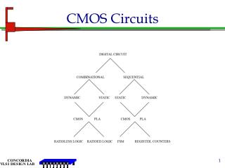
CMOS Circuits. Combination and Sequential. VDD. PMOS. Network. Output. Inputs. NMOS. Network. Static Combinational Network. CMOS Circuits Pull-up network-PMOS Pull-down network- NMOS Networks are complementary to each other

CMOS Circuits
E N D
Presentation Transcript
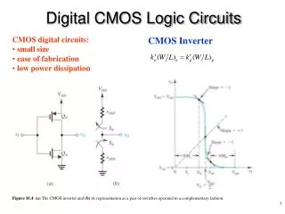
VDD PMOS Network Output Inputs NMOS Network Static Combinational Network • CMOS Circuits • Pull-up network-PMOS • Pull-down network- NMOS • Networks are complementary to each other • When the circuit is dormant, no current flows between supply lines. • Number of the NMOS transistors (PMOS transistors) equals to the number of the inputs. • Output load is capacitive
NAND Gates Transistors in Parallel 1/Rcheff = (1/Rch1) + (1/Rch2) Transistors in Series Rcheff = Rch1 + Rch2
CMOS NAND Gate DC Analysis Two possible scenarios: 1. Both inputs are toggling 2. One input is toggling, the other one set high Assumptions: MP2=MP1=MP MN1=MN2=MN W/L for MP = (W/L)p W/L for MN = (W/L)n Inverter VTC
Gate Sizing To obtain equal Rise and Fall time, Size the series / parallel transistors to have an equivalent of a single PU or PD inverter transistor in your design
NAND Gates: Analysis Scenario #1- Both inputs are toggling L-H > (W/L)eff = 2(W/L)p H-L > (W/L)eff = 1/2(W/L)n KR|NAND = 1/4 KR|INV Scenario #2- One input is toggling L-H > (W/L)eff = (W/L)p H-L > (W/L)eff = 1/2(W/L)n KR|NAND = 1/2 KR|INV Vin Inverter One input toggling V OH Two inputs toggling Vin=Vout V OL Vout Vx2 Vx1
NAND Gates: Analysis Switching Analysis Scenario #1- Both inputs are toggling tPLH |NAND = 1/2tPLH |INVERTER tPHL |NAND = 2tPHL |INVERTER Scenario #2- One input is toggling tPLH |NAND = tPLH |INVERTER tPHL |NAND = 2tPHL |INVERTER
NAND Gate: Power Dissipation Pac= α.f . C VDD2 A B X 0 0 1 1 0 1 0 1 1 1 1 0 α= P (X=1). P (X=0) assuming A and B have equal probabilities for 1 and 0 α = (1/4). (3/4)= 3/16 C = CL + C parasitic
NOR Gate: Analysis DC Analysis/ AC Analysis Two possible scenarios: 1. Both inputs are toggling (one is set low) 2. One input is toggling, the other one set high Assumptions: AP2=BP1=MP AN1=BN2=MN W/L for MP = (W/L)p W/L for MN = (W/L)n Compare with a CMOS inverter: MP/MN KR, and the shift in VTC Propagation delay tPLH andtPHL
VDD A B C D X B C A C D L 4 INPUT NOR Gate Very slow rise time and rise delays Could be compensated by increasing of PMOS transistor size. Implications: Silicon Area Input capacitance
Practical Considerations 1. Minimize the use of NOR gates 2. Minimize the fan-in of NOR gates 3. Limit the fan-in to 4 for NAND gates 4. Use De morgan’s theorem to reduce the number of fan-in per gate Example:
Pseudo nMOS NAND/NOR Gates From Lecture #4 For acceptable operation WN=1.5 WP for our Process respecting min WP
Pseudo nMOS Complex Gates From Lecture #4 For acceptable operation WN=1.5 WP for our Process respecting min WP
CASCODE LOGIC Lad is cross coupled pMOS transistors Logic is series and parallel complementary transistors Input and Output are in Complementary forms
DCVS trees for a full adder Sum and Carry Pull-Down Networks S’(A,B,C) = A’BC’ + A’B’C + ABC + AB’C’ S (A,B,C) = A’B’C’ + A’BC + ABC’ + AB’C C(A,B,C) = AB + BC + AC
Transmission Gate Bi-directional switch, passes digital signals Less complex and more versatile than AND gate Passes analog signals Problems: Large ON resistance during transitions of input signals Large input and output capacitance (useful for data storage applications) Capacitive coupling Applications: Multiplexers, encoders, latches, registers various combinational logic circuits C A B C
NMOS/PMOS as Pass Transistors NMOS Transistor Passes weak “1” signal Vo = VDD -VTN Passes “0” signal undegraded C Vo VDD -VTN Vi Vo CL VDD -VTN Vi PMOS Transistor Passes “1” signal undegraded Passes weak “0” signal Vo= -VTP Vo C Vi Vo -VTP CL Vi -VTP
Vo Vin nmos:lin nmos:sat nmos:off pmos:sat pmos:lin pmos:lin 0V |VTP| VDD-VTN VDD TX Gate: Characteristics 0
TX Gate: Layout C VDD P+ P+ Vi VO N+ N+ C VSS C C For data path structure
NAND Gates: Layout Layout Transistors in Series Transistors in Parallel
NAND Gates: Layout VDD Via Metal II X A B GND
NOR Gate: Layout VDD X B A GND
p+ layer contact n+ layer active polysilicon metal (diffusion) Analysis and Design of Complex Gate Analysis 1. Construct the schematic 2. Determine the logic function. 3. Determine transistor sizes. 4. Determine the input pattern to cause slowest and fastest operations. 5. Determine the worst case rise delay (tPLH)and fall delay (tPHL) 6. Determine the best case rise and fall delays. A B C D E F VDD OUT N-well GND A B C D E F

