CMOS Logic Circuits
CMOS Logic Circuits. Logic Values. Logic values = {0, 1} A logic value, 0 or 1, is called as BI nary Digi T or BIT . Physical states representing bits in digital technologies:. Encoding Bits. Information can be encoded using: Current, Voltage, Phase, Frequency


CMOS Logic Circuits
E N D
Presentation Transcript
CMOS Logic Circuits
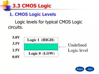
Logic Values • Logic values = {0, 1} • A logic value, 0 or 1, is called asBInary DigiTor BIT. • Physical states representing bits in digital technologies:
Encoding Bits • Information can be encoded using: • Current, Voltage, Phase, Frequency • Digital systems use two voltage levels for encoding bits. • LOW: A signal close to the GND • HIGH: A signal close to the VCC
Encoding Bits • Positive logic • High: 1 and Low: 0 • Our convention in this course • Negative logic • High: 0 and Low: 1
Logic Gates • Gates are basic digital devices. • A gate takes one or more inputs and produces an output. • Inputs are either 0 or 1. • Although they may have very different values of voltage. • Output is either 0 or 1. • A logic gate’s operation is fully described by a truth table.
Logic Families – What is inside of a logic gate? • A logic family is a collection of different integrated-circuit chips that have similar input, output, and internal circuit characteristics, but that perform different logic functions. • Logic gates are made from transistors. • TTL (Transistor-Transistor Logic) family gates are made from bipolar transistors. • CMOS (Complementary Metal Oxide Semiconductor) family logic gates are made from MOS transistors.
MOS Transistors – N-type MOSFET • OFF (open circuit) :when gate is logical zero • ON (short circuit) :when gate is logical one • Passes a good logical zero • Degrades a logical one
MOS Transistors – P-type MOSFET • OFF (open circuit) :when gate is logical one • ON (short circuit) :when gate is logical zero • Passes a good logical one • Degrades a logical zero
CMOS Electrical Characteristics • Digital analysis works only if circuits are operated in specs: • Power supply voltage • Temperature • Input-signal quality • Output loading • Must do some “analog” analysis to prove that circuits are operated in spec. • Fan-out specs • Timing analysis (setup and hold times) • Analysis involves only consequences of V = IR (static) and q = CV (dynamic)
CMOS Electrical Characteristics • Logic voltage levels • DC noise margin • Fan-in • Fan-out • Speed • Power consumption
Logic Levels • Typical transfer characteristic of a CMOS inverter: • LOW input level: < 2.4 Volt • HIGH input level: > 2.6 Volt • Transfer characteristic depends on power-supply voltage, temperature and output loading.
Logic Levels • Should use more conservative specifications for LOW and HIGH • VILmax: max input voltage guaranteed to be recognized as a LOW level • 30% of VCC • VOLmax: max output voltage in the LOW level • GND + 0.1 V • VOHmin: min output voltage in the HIGH level • VCC – 0.1 V • VIHmin: min input voltage guaranteed to be recognized as a HIGH level • 70% of VCC
Logic Levels VILmax VIHmin VOLmax VOHmin
DC Noise Margins • DC noise margin is a measure of how much noise it takes to corrupt a worst-case output voltage into a value that may not be recognized properly by an input. • Noise Margin Low = VILmax – VOLmax = 1.35– 0.1 = 1.25 V • Noise Margin High = VOHmin – VIHmin = 4.4– 3.15 = 1.25 V
Input Currents • CMOS gate inputs consume very little current, only the leakage current of the two transistors’ gates. • IIH: max current that flows into the input in HIGH state • IIL: max current that flows into the input in LOW state
DC Output Loading • An output must sink current from a load when the output is in the LOW state. • An output must source current to a load when the output is in the HIGH state.
DC Output Loading Specs • VOLmax and VOHmin are specified for certain output-current values, IOLmax and IOHmax. • IOLmax: max current that output can sink in the LOW state while still maintaining an output voltage no greater than VOLmax • IOHmax: max current that output can source in the HIGH state while still maintaining an output voltage no less than VOHmin
DC Output Loading - Output-voltage Drops • Resistance of “off” transistor is > 1 Megaohm, but resistance of “on” transistor is nonzero, • Voltage drops across “on” transistor, V = IR • For “CMOS” loads, current and voltage drop are negligible. • For TTL inputs, LEDs, terminations, or other resistive loads, current and voltage drop are significant and must be calculated. • If too much load, output voltage will go outside of valid logic-voltage range. • VOHmin, VIHmin • VOLmax, VILmax
Fan-in • The number of inputs that a gate can have in a particular logic family is called the logic family’s fan-in. • You could design a CMOS NAND or NOR gates with a very large number of inputs. • In practice, additive “on” resistance of series transistors limits the fan-in of CMOS gates – Lower speed. • Max fan-in = 4 for NOR, 6 for NAND 7-input NAND gate using 4-input NAND gates 3-input NAND gate
Fan-out • The fan-out of a gate is the number of inputs that the gate can drive without exceeding its worst-case loading specifications. • Characteristics of the gate’s output • Characteristics of the inputs that it is driving • DC fan-out: The number of inputs that an output can drive with the output in a constant state (high or low). • AC fan-out: The ability of an output to charge or discharge the stray capacitance associated with the inputs that it drives. • If the capacitance is too large, the transition from low to high (or vice versa) may be too slow, causing improper system operation.
DC Fan-out Calculation • LOW state: The sum of the IIL values of the driven inputs may not exceed IOLmax of the driving output. • HIGH state: The sum of the IIH values of the driven inputs may not exceed IOHmax of the driving output. Low State Fan-out= 20 μA/1 μA= 20 High State Fan-out= 20 μA/1 μA= 20
AC Loading • AC loading has become a critical design factor as industry has moved to pure CMOS systems. • CMOS inputs have very high impedance, DC loading is frequently negligible (low fan-outs). • CMOS inputs and related packaging and wiring have significant capacitance. • Time to charge and discharge capacitance is a major component of delay. • Gate’s speed and power consumption depend on the AC characteristics of the gate and its load.
Transition Time • The amount of time that the output of a logic circuit takes to change from one state to another is called the transition time. • tR : rise time – time to chage from low to high • tF : fall time – time to chage from high to low
Transition Time • The rise and fall times of a CMOS output depend mainly on • “on” transistor resistance • capacitive load • Capacitive load = Stray capacitance = AC load • Output circuits: A gate’s output transistors, internal wiring, packaging • The wiring that connects an output to other inputs • Input circuits: A gate’s input transistors, internal wiring, packaging
Propagation Delay • The propagation delay is the amount of time that it takes for a change in the input signal to produce a change in the output signal. • tPHL : high-to-low propogation time • tPLH : low-to-high propogation time • tPD : propogation delay; tPD= max (tPHL, tPLH) • tPD determines the gate speed
Power Consumption • Static power consumption: Power consumption when the circuit’s output is not changing • Very low static power consumption for CMOS circuits • Attractive for low-power applications • Power consumption due to the leakage currents • Dynamic power consumption: Power consumption when the circuit’s output is in transition PD = (CPD + CL) x (VCC)2 x f • PT : Dynamic power consumption • VCC: Power-supply voltage • f: Transition frequency of the output signal • CPD : Power-dissipation capacitance – Specified by the device manufacturer and around 20-24 pF • CL : Load capacitance
CMOS Logic Family • 4000 series • First commercially successful CMOS family • Fairly slow and not easy to interface to TTL • CMOS device part number: 74FAMnn or 54FAMnn • HC/HCT: High speed CMOS/ High speed CMOS, TTL compatible • FCT/FCT-T: Fast CMOS/ Fast CMOS, TTL compatible • VHC/VHCT: Very high speed CMOS/ Very high speed CMOS, TTL compatible
CMOS-TTL Interface • DC noise margin • CMOS outputs driving TTL inputs: Ok • TTL outputs driving CMOS inputs: CMOS device must be HCT, VHCT or FCT • Fan-out • TTL outputs driving CMOS inputs: Ok • CMOS outputs driving TTL inputs: Limited • Capacitive loading • Increasing delay and power consumption • All CMOS families have similar dynamic power consumption • TTL outputs have lower dynamic power consumption