CMOS Logic Circuits
CMOS Logic Circuits. Inverter 2 Input NOR 2 Input NAND Other functions. V dd = 5V. V out. V in. T pu (pMOS). T pd (nMOS). The CMOS Inverter. V(x). V(y). V(y)=V(x). Switching Threshold. V M. DC Operation Voltage Transfer Characteristics (VTC).


CMOS Logic Circuits
E N D
Presentation Transcript
CMOS Logic Circuits Inverter 2 Input NOR 2 Input NAND Other functions
Vdd = 5V Vout Vin Tpu (pMOS) Tpd (nMOS) The CMOS Inverter
V(x) V(y) V(y)=V(x) Switching Threshold VM DC Operation Voltage Transfer Characteristics (VTC) • Plot of output voltage as a function of the input voltage V(y) f VOH = f (VIL) VOL = f (VIH) VIL VIH V(x)
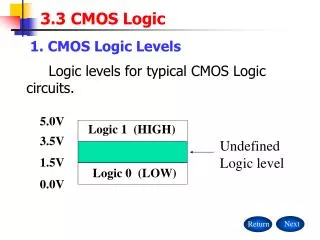
VOH "1" VIH Undefined Region VIL VOL "0" Mapping Logic Levels to the Voltage Domain • The regions of acceptable high and low voltages are delimited by VIH and VIL that represent the points on the VTC curve where the gain = -1 V(y) Slope = -1 VOH Slope = -1 VOL VIL VIH V(x)
Fan-out – number of load gates connected to the output of the driving gate • gates with large fan-out are slower N • Fan-in – the number of inputs to the gate • gates with large fan-in are bigger and slower M Fan-In and Fan-Out
The Ideal Inverter • The ideal gate should have • infinite gain in the transition region • a gate threshold located in the middle of the logic swing • high and low noise margins equal to half the swing • input and output impedances of infinity and zero, resp. Vout Ri = Ro = 0 Fanout = NMH = NML = VDD/2 g = - Vin
n-FET p-FET gate transmission gate NOR inverter NAND B (AB) A B (A+B) A TG CMOS Logic Gates • CMOS integrated circuits are built around using two kinds of Field Effect Transistors (FET), n-type & p-type. • the gate input controls whether current can flow between the other two terminals or not. • Logic gates are constructed by combining transistors in complementary arrangements.
X Y Z X Y Z Circuit Delays in CMOS Circuits • Electronic gates are physical devicesthat take time to operate. • Response to instantaneous change atX is gradual decrease in voltage atY and similar gradual increase at Z. • Voltage at Y must drop below logicthreshold level to be “seen” as a ‘0’. • This effect can be viewed as delay in propagation of logic values. • tPLH denotes low-to-high delay • tPHL denotes high-to-low delay • tpd= max{tPLH, tPHL} • relative values of tPLH and tPHL depend on relative “strength” of pull-up and pull-down transistors in inverters • values vary with operating temperature and manufacturing processes
equivalent circuitwhen X is low X Y Z Z Y X X Y Z equivalent circuitwhen X is high X Y Z Closer Look at CMOS Circuit Delays • Decrease of voltage at Y requires transfer of charge from capacitor to ground. • wires and transistor gates act like capacitors • time for transfer depends on size of capacitance and on resistance of pull-down transistor • pull-up & pull-down transistors can have different “on-state” resistance values • Use of two parallel inverters between X and Y can give faster logic transitions. • When X goes high, pull-up of first inverter turns off and pull-down turns on.
VDD Vin Vout CL Circuit: The CMOS Inverter
CMOS Inverter - Operation Since the gate is essentially an open circuit it draws no current, and the output voltage will be equal to either ground or to the power supply voltage, depending on which transistor is conducting. When input A is grounded (logic 0), the N-channel MOSFET is unbiased, and therefore has no channel enhanced within itself. It is an open circuit, and therefore leaves the output line disconnected from ground. At the same time, the P-channel MOSFET is forward biased, so it has a channel enhanced within itself, connecting the output line to the +Vsupply. This pulls the output up to +V (logic 1). When input A is at +V (logic 1), the P-channel MOSFET is off and the N-channel MOSFET is on, thus pulling the output down to ground (logic 0). Thus, this circuit correctly performs logic inversion, and at the same time provides active pull-up and pull-down, according to the output state.
The CMOS Inverter (mask layout) & SPICE simulation In Out Time • In 0.25µm typical delay 50ps
CMOS Inverter (Recall) Inverter Layout Using Microwind
+V Y = A + B A B CMOS 2-Input NOR
CMOS 2-Input NOR - Operation This basic CMOS inverter can be expanded into NOR and NAND structures by combining inverters in a partially series, partially parallel structure. A practical example of a CMOS 2-input NOR gate is shown in the figure. In this circuit, if both inputs are low, both P-channel MOSFETs will be turned on, thus providing a connection to +V. Both N-channel MOSFETs will be off, so there will be no ground connection. However, if either input goes high, that P-channel MOSFET will turn off and disconnect the output from +V, while that N-channel MOSFET will turn on, thus grounding the output. Note the two p-channel FETs in series.
+V +V A B Y = A • B CMOS 2-Input NAND
p A p B out n n 2-Input NAND If both inputs 1, both p-channel are off, both n-channel are on, out is negative; otherwise at least one p-channel is on and one n-channel off, and out is positive
CMOS 2-Input NAND - Operation A two-input NAND gate: a logic 0 at either input will force the output to logic 1; both inputs at logic 1 will force the output to go to logic 0. Note the two n-channel FETs in series and the two p-channel FETs in parallel. The pull-up and pull-down resistances at the output are never the same, and can change significantly as the inputs change state, even if the output does not change logic states. The result is uneven and unpredictable rise and fall times for the output signal. This problem was addressed, and was solved with the buffered, or B-series CMOS gates.
+V +V Y = A • B B CMOS 2-Input NAND: Buffered
CMOS 2-Input NAND: Buffered The technique here is to follow the actual NAND gate with a pair of inverters. Thus, the output will always be driven by a single transistor, either P-channel or N-channel. Since they are as closely matched as possible, the output resistance of the gate will always be the same, and signal behavior is therefore more predictable. Typically, the p-channel transistor is approximately twice as wide as the n-channel transistor, because of the difference in conductivity between electronics and holes. Note that we have not gone into all of the details of CMOS gate construction here. For example, to avoid damage caused by static electricity, different manufacturers developed a number of input protection circuits, to prevent input voltages from becoming too high. However, these protection circuits do not affect the logical behavior of the gates, so we will not go into the details here. This is not strictly true for most CMOS devices for applications that are power-switched; special inputs are required for power-off isolation between circuits.
CMOS 2-Input XOR Layout of 2 Input XOR Using Microwind