
Basic Register
E N D
Presentation Transcript
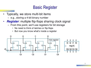
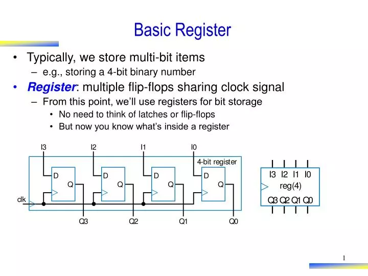
Basic Register • Typically, we store multi-bit items • e.g., storing a 4-bit binary number • Register: multiple flip-flops sharing clock signal • From this point, we’ll use registers for bit storage • No need to think of latches or flip-flops • But now you know what’s inside a register
Present 1 hour ago 2 hours ago Display Display Display b4 b3 b2 b1 b0 c4 c3 c2 c1 c0 a4 a3 a2 a1 a0 x4 e x3 r tu x2 a r Temperature History Storage x1 sensor x0 empe t timer C Example Using Registers: Temperature Display • Temperature history display • Sensor outputs temperature as 5-bit binary number • Timer pulses C every hour • Record temperature on each pulse, display last three recorded values (In practice, we would actually avoid connecting the timer output C to a clock input, instead only connecting an oscillator output to a clock input.)
a4 a3 a2 a1 a0 b4 b3 b2 b1 b0 c4 c3 c2 c1 c0 I 4 Q4 I 4 Q4 I 4 Q4 x4 I 3 Q3 I 3 Q3 I 3 Q3 x3 I 2 Q2 I 2 Q2 I 2 Q2 x2 I 1 Q1 I 1 Q1 I 1 Q1 x1 I 0 Q0 I 0 Q0 I 0 Q0 x0 R a R b R c C Temperature History Storage 15 18 20 21 21 22 24 24 24 25 25 26 26 26 27 27 27 27 x4...x0 C 0 18 21 24 25 26 27 R a R b 0 0 18 21 24 25 26 R c 0 0 0 18 21 24 25 Example Using Registers: Temperature Display • Use three 5-bit registers
b Controller laser x clk patient Finite-State Machines (FSMs) and Controllers • Want sequential circuit with particular behavior over time • Example: Laser timer • Push button: x=1 for 3 clock cycles • How? Let’s try three flip-flops • b=1 gets stored in first D flip-flop • Then 2nd flip-flop on next cycle, then 3rd flip-flop on next • OR the three flip-flop outputs, so x should be 1 for three cycles
Need a Better Way to Design Sequential Circuits • Trial and error is not a good design method • Combinational circuit design process had two important things • A formal way to describe desired circuit behavior • Boolean equation, or truth table • A well-defined process to convert that behavior to a circuit • We need those things for sequence circuit design
Outputs: x clk ^ x=0 x=1 O ff On clk ^ Describing Behavior of Sequential Circuit: FSM • Finite-State Machine (FSM) • A way to describe desired behavior of sequential circuit • Akin to Boolean equations for combinational behavior • List states, and transitions among states • Example: Make x change toggle (0 to 1, or 1 to 0) every clock cycle • Two states: “Off” (x=0), and “On” (x=1) • Transition from Off to On, or On to Off, on rising clock edge • Arrow with no starting state points to initial state (when circuit first starts)
Outputs: x clk ^ clk ^ clk ^ x=0 x=1 x=1 x=1 O ff On1 On2 On3 clk ^ clk O ff On1 On2 On3 O ff On1 On2 On3 O ff State Outputs: x FSM Example: 0,1,1,1,repeat • Want 0, 1, 1, 1, 0, 1, 1, 1, ... • Each value for one clock cycle • Can describe as FSM • Four states • Transition on rising clock edge to next state
Inputs: b; Outputs: x x=0 clk ^ O ff ^ b ’*clk b*clk ^ clk clk ^ ^ x=1 x=1 x=1 On1 On2 On3 Extend FSM to Three-Cycles High Laser Timer • Four states • Wait in “Off” state while b is 0 (b’) • When b is 1 (and rising clock edge), transition to On1 • Sets x=1 • On next two clock edges, transition to On2, then On3, which also set x=1 • So x=1 for three cycles after button pressed
Inputs: b; Outputs: x x=0 clk ^ O ff ^ b’ *clk b *clk ^ clk clk ^ ^ x=1 x=1 x=1 On1 On2 On3 Inputs: x; Outputs: b x=0 Off b ’ b x=1 x=1 x=1 On1 On2 On3 FSM Simplification: Rising Clock Edges Implicit • Showing rising clock on every transition: cluttered • Make implicit -- assume every edge has rising clock, even if not shown • What if we wanted a transition without a rising edge • We don’t consider such asynchronous FSMs -- less common, and advanced topic • Only consider synchronous FSMs -- rising edge on every transition Note: Transition with no associated condition thus transistions to next state on next clock cycle
Inputs: x; Outputs: b x=0 Off b ’ b x=1 x=1 x=1 On1 On2 On3 FSM Definition • FSM consists of • Set of states • Ex: {Off, On1, On2, On3} • Set of inputs, set of outputs • Ex: Inputs: {x}, Outputs: {b} • Initial state • Ex: “Off” • Set of transitions • Describes next states • Ex: Has 5 transitions • Set of actions • Sets outputs while in states • Ex: x=0, x=1, x=1, and x=1 We often draw FSM graphically, known as state diagram Can also use table (state table), or textual languages
Inputs: a; Outputs: r Wait r=0 a ’ a K1 K2 K3 K4 r=1 r=1 r=0 r=1 FSM Example: Secure Car Key • Many new car keys include tiny computer chip • When car starts, car’s computer (under engine hood) requests identifier from key • Key transmits identifier • If not, computer shuts off car • FSM • Wait until computer requests ID (a=1) • Transmit ID (in this case, 1101)
I nputs: a ; O utputs: r W ait r=0 a ’ a K1 K2 K3 K4 r=1 r=1 r=0 r=1 clk I nputs a clk I nputs State W ait W ait K1 K2 K3 K4 W ait a S t a t e W ait W ait K1 K2 K3 K4 W ait W ait Output r O utputs r FSM Example: Secure Car Key (cont.) • Nice feature of FSM • Can evaluate output behavior for different input sequence • Timing diagrams show states and output values for different input waveforms Q: Determine states and r value for given input waveform: K1
Inputs: s,r,g,b,a; Outputs: u Wait u=0 s ’ s a r ’ a b ’ a g ’ a r ’ Start a ’ u=0 ar ag ab ar Red1 Blue Green R ed2 a ’ a ’ a ’ u=0 u=0 u=0 u=1 FSM Example: Code Detector • Unlock door (u=1) only when buttons pressed in sequence: • start, then red, blue, green, red • Input from each button: s, r, g, b • Also, output a indicates that some colored button pressed • FSM • Wait for start (s=1) in “Wait” • Once started (“Start”) • If see red, go to “Red1” • Then, if see blue, go to “Blue” • Then, if see green, go to “Green” • Then, if see red, go to “Red2” • In that state, open the door (u=1) • Wrong button at any step, return to “Wait”, without opening door s Start u r Door Red Code g lock detector Green b Blue a Q: Can you trick this FSM to open the door, without knowing the code? A: Yes, hold all buttons simultaneously
Improve FSM for Code Detector • New transition conditions detect if wrong button pressed, returns to “Wait” • FSM provides formal, concrete means to accurately define desired behavior Inputs: s,r,g,b,a; Outputs: u Wait ar’ ab’ ag’ ar’ s’ u=0 s Start a ’ u=0 ar ag ar ab Red1 Blue Green Red2 a ’ a ’ a ’ u=0 u=0 u=0 u=1
Inputs: x; Outputs: b x=0 Off b ’ b x=1 x=1 x=1 On1 On2 On3 outputs FSM inputs x FSM b FSM outputs Combinational logic n1 FSM inputs O I FSM outputs n0 Combinational logic s1 s0 S State register clk m m m-bit state register clk N General version Standard Controller Architecture • How implement FSM as sequential circuit? • Use standard architecture • State register -- to store the present state • Combinational logic -- to compute outputs, and next state • For laser timer FSM • 2-bit state register, can represent four states • Input b, output x • Known as controller