Download
1 / 43
430 likes | 619 Vues
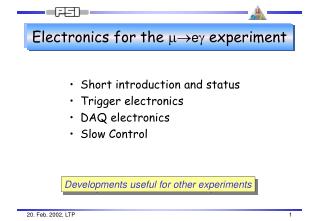
Electronics for the m e g experiment. Short introduction and status Trigger electronics DAQ electronics Slow Control. Developments useful for other experiments. Kinematics. q e g = 180°. m. e. g. E e = 52.8 MeV. E g = 52.8 MeV. Search for m e g at 10 -14.

E N D
Electronics for the meg experiment • Short introduction and status • Trigger electronics • DAQ electronics • Slow Control Developments useful for other experiments
Kinematics qeg= 180° m e g Ee = 52.8 MeV Eg = 52.8 MeV Search for meg at 10-14 • LFV Process forbidden by SM • n oscillations expected to enhance LFV rate • Present limit: 1.2 • 10-11 (MEGA) • SUSY Theories: ~ 10-12 • Required: • m+ stopping rate: 108/s • Resolutions (all FWHM): • DEe: 0.7% • DEg: 1.4% @ 52.8 MeV • Dqeg: 12 mrad • Dteg: 150ps MEG Detector
Detector Design Tests & Design 2002 Assembly 2003 Engineering Run 2004 2005 Data taking 2006 2007 . . .
Status update • New xenon purification with SAES mono-torr getter filter. Should reduce all non-noble gases to < ppb level • Very low noise on PMTs (1mV peak-to-peak) 0.2% resolution when summing all 240 PMTs • PMT gain equalized reproducible with LED method to ~3%, limited by HV stability • Beam time at TERAS starts today
Kinematics qeg= 180° g m e g e + Ee = 52.8 MeV Eg = 52.8 MeV Trigger Requirements • Beam rate 108 s-1 • Fast LXe energy sum > 45MeV 2103 s-1 • g interaction point • e+ hit point in timing counter • time correlation g – e+ 200 s-1 • angular corrlation g – e+ 20 s-1 M.C.
LXe energy sum • Total ~800 PMTs • Common noise contributes significantly to analog sum • AC coupling Baseline drift • How to evaluate q,f of shower center?
Digital Trigger • Commodity electronics available • 100 MHz FADC 10 bit (10$) • FPGA 100k Gates, 90kB, 230 MHz, 300 pins (100$) • SRAM 10ns, 128kB (30$) • LVDS 200Mb/s/line, (2$) • VME32/VME64 FADC PMT FADC PMT FPGA Trigger FADC SRAM PMT …
Baseline Subtraction Baseline Subtraction 100 MHz Clock 10 bit Latch Latch Latch Latch Calibrated and linearized signal Baseline subtracted signal + Latch LUT 10x10 S - S S - + Uses ~120 out of 5000 logic cells 8 channels/FPGA use 20% of chip S S Latch Baseline Register <thr
QT Algorithm original waveform t • Inspired by H1 Fast Track Trigger (A. Schnöning) • Difference of Samples (= 1st derivation) • Hit region defined when DOS is above threshold • Integration of original signal in hit region • Pedestal evaluated in region before hit • Time interpolated using maximum value and two neighbor values in LUT 1ns resolution for 10ns sampling time Region for pedestal evaluation integration area smoothed and differentiated (Difference Of Samples) Threshold in DOS
Dq Dj Finding center of g shower ε (|φ(center)-j(max. PMT)| < 3.5°) > 99% Enough to find PMT with max. value
Schema for max. finding 8 Latch 8 index LSB 8 Latch Index bit A A<B MSB Latch B 8 value Latch 8 Index bit Latch A A>B 8 B Latch Index bit 8 A A<B B
LXe Sum > 45MeV Trigger AND g phi max PMT LUT LUT back-to back other veto e+ counter e+ phi LUT or or or e+ - g coincidence
Trigger latency ADC BS S ADC BS S >45MeV ADC BS S ADC BS . . . AND . . . . . . Max Max Df Max fe+ 10 stages = 1024 chn T[ns] 0 50 100 110 120..200 220 230
VME Boards Type1 Type2 FADC 3.3V 2.5V VME Interface (Cypress) LVDS 3.3V 2.5V VME Interface (Cypress) FADC LVDS 8 channels FADC FPGA LVDS FPGA FADC LVDS FADC FPGA LVDS FPGA SRAM SRAM FADC LVDS 8 channels FADC LVDS FADC LVDS FPGA SRAM FPGA SRAM LVDS LVDS FPGA LVDS FPGA LVDS LVDS LVDS LVDS LVDS LVDS clck, clear 48 bits output
Board hierarchy • 42 Type 1 boards for 600 channels • 6 Type 2 boards (VME 9U) • 3 VME crates (2x6U, 2x9U) • Total latency 350ns • Processing power 600 * 100 MHz * 10 bit = 75 GB/s • “Golden Rule”: plan for FPGAs with 2x gates • Totally re-programmable • Estimated costs: 230k$ • Made by INFN, Pisa
Prototype board Peter Dick FPGA Signal- Generator ADC DAC
m e DAQ Hardware Requirements n PMT sum 0.511 MeV meg Michel edge 51.5 MeV 50 51 52 E[MeV] t ~100ns (menn)2 + g • g’s hitting different parts of LXe can be separated if > 2 PMTs apart (15 cm) • Timely separated g’s need waveform digitizing > 300 MHz • If waveform digitizing gives timing <100ps, no TDCs are needed g e m
Fast waveform Digitizing • Trigger boards can directly be used for Drift Chamber (10ns sampling 1ns interpolation 2-3ns chamber resolution) • Waveforms stored in SRAM, sparcified readout via LVDS • Calorimeter readout needs sampling with > 1GHz FADC 3.3V 2.5V VME Interface (Cypress) FADC 8 channels FADC FPGA FADC FADC FPGA SRAM FADC 8 channels FADC FADC FPGA SRAM 2GHz 40MHz, 12 bit FPGA DSC FADC FPGA LVDS Analog Waveform Domino Sampling Chip SRAM LVDS LVDS clck, clear 48 bits output
pb Domino Sampling Chip • 0.5 – 1.2 GHz sampling speed • 128 sampling cells • Readout at 5 MHz, 12 bit • ~ 100 CHF/channel • Needed: • 2.5 GHz sampling speed • Circular domino wave • 1024 sampling cells • 40 MHz readout • < 100ps accuracy
input Domino Ring Sampler (DRS) • Free running domino wave, stopped with trigger • Sampling speed 2 GHz (500ps/bin) • Readout 40 MHz 12 bit • 1024 bins 150ns waveform + 350ns delay
Domino Cell domino enable • “Tail-biting” mechanism to chop off domino wave • Coupling in of Domino Start in all cells for homogeneity • Minimal number of components in critical path • Global Domino Enable • Capacitor to slow down speed
Domino Wave stability NMOS<PMOS w/o tail biting NMOS<PMOS with tail-biting NMOS=PMOS “starving” widened stable
Gate sampling signal • Domino stop only accurate by one cell (500ps) • Need 50ps timing resolution Trigger gate sampling trigger gate 500ps 50ps
DAQ Board • 9 channels 1024 bins / 40 MHz = 230 ms acceptable dead time • Zero suppression in FPGA • QT Algorithm in FPGA (store waveform if multi-hit) • Readout controller in FPGA(instead pattern generator) 8 channel DRS 3.3V 2.5V VME Interface (Cypress) 40 MHz 12 bit 8 channel DRS FPGA FADC 8 inputs FADC 8 channel DRS SRAM FPGA 8 channel DRS FPGA FADC SRAM Trigger Input SRAM shift register trigger gate 3 state switches Board inter-connect SRAM SRAM Trigger BUS (2nd level tr.)
Status DRS • Simulation finished in AMS 0.35m process • Layout started • Switch to 0.25m process • First version summer ’02 • Readout with trigger prototype board • Costs per channel:~25$ (board) + 6$ (chip)
DAQ Muegamma Split and Preamplifier Trigger Board LXe e+ PMT trigger DSC FADC FPGA CPU 40MHz 2GHz Waveform or QT readout DAQ board optional 2nd level trigger trigger CPU Trigger Board wires strips 100MHz DC Waveform or QT readout
TDC Disc. Scaler ADC Scope “Redefinition” of DAQ DSC ~GHz FADC 100 MHz FPGA SRAM
Applications in other experiments • Technology in house (pool) • Substitution of old electronics (ADC, Scaler, Discriminators) • LVDS-NIM converter and VME necessary • Integration in new experiments Beam Counters FADC 3.3V 2.5V VME Interface (Cypress) PMT Dttrigger= 10ns DtTDC 1ns FADC PMT FADC FPGA PMT FADC FADC FPGA SRAM FADC calorimeter FADC FADC FPGA SRAM FPGA LVDS LVDS LVDS
PC 12:30 12.3 12:45 17.2 13:20 15.2 14:10 17.3 15:20 16.2 18:30 21.3 19:20 18.2 19:45 19.2 Slow Control HV Temperature, pressure, … Valves 12345 Terminal Server PLC RS232 GPIB ??? 15° C Ethernet heater MIDAS DAQ
Slow Control Bus HV Temperature, pressure, … Valves heater MIDAS DAQ
LXe calorimeter HV requirements • 12 stage bases @ 1000V • Dg = (DU)12 1V accuracy = 1.2% gain variation • Need <0.3V accuracy over full temperature range • Low ripple • 1000 channels ~ 200k$ commercially • Fast readout for monitoring (RS232 would take ~3 min to read)
CAN, Profibus, LON available Node with ADC ~100$ Interoperatibility not guaranteed Protocol overhead Local CPU? User programmable? How to integrate in HV (CAEN use CAENET) Field Bus Solutions Reinhard Schmidt
RS485 bus • Similar to RS-232 but • Up to 256 (1/8 load) units can be connected to a single segment • single line, half duplex • differential twisted pair • Segment length up to km • MAX 1483 transceiver chip for HV control • MAX 1480 for opto decoupled applications • Use repeater to extend to many segments
ADuC812 / C8051F000 Microcontrollers MAX 1483 Tranceiver Flat ribbon connector Power through bus Costs ~30$ Piggy back board Generic Node
Generic node with signal conditioning (OP-AMPs) Sub-master with power supply and PC connection (Parallel Port, USB planned) Integration on sensors, in crates RS232 node planned 2 versions BUS Oriented Crate Oriented • 19” crate with custom backplane • Generic node as piggy-back • Cards for analog IO / digital IO / temperature / 220V / … • Crate connects to parallel port (USB planned)
Protocol • Asynchronous 345 kBaud • 16-bit addressing (65536 nodes) • CRC-code for error detection • Optional acknowledge • Concept of channels and configuration parameters (256 each per node) address command node command LSB MSB CRC channel1 param1 ADC 1 Byte channel2 param2 ADC write data param3 channel3 command channel value CRC port
Midas Slow Control Bus • 256 nodes, 65536 with one level of repeaters • Bus length ~500m opto-isolated • Boards for voltage, current, thermo couples, voltage output, TTL IO, 220V output, available from pool on request • Readout speed: 0.3s for 1000 channels • C library, command-line utility, Midas driver, LabView driver • Connects to parallel port, USB planned • Nodes are “self-documenting” • Configuration parameters in EEPROM on node • Node CPU can operate autonomously for interlock and regulation (PID) tasks (C programmable) • Nodes can be reprogrammed over network http://midas.psi.ch/mscb
LabView Logger • Used for POLDI detector HV and gas monitoring • Graph, logging and alarm notification
Regulates common HV source 0-2400V, ~1mA DAC 16bit, ADC 14bit Current trip ~10ms Self-calibration with two high accuracy reference voltages Accuracy <0.3V absolute Boards with 12 channels, crates with 192 channels 30$/channel HV performance Prototype
Conclusions • Lots of new electronics for Muegamma • Can be useful for other experiments • Knowledge and support in-house • Open to suggestions and modifications Credits to Reinhard Schmidt and Peter Dick
Muegamma Web Site Transparencies: http://meg.psi.ch/doc/talks/s_ritt/feb02_psi Cake: http://kochbuch.unix-ag.uni-kl.de/bin/rezept?17731