Microfabrication Techniques for Accelerators
220 likes | 239 Vues
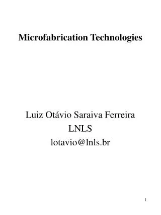
Microfabrication Techniques for Accelerators. A. Nassiri, R.L. Kustom, D.C. Mancini Argonne National Laboratory. Symposium in Memory of Robert H. Siemann and ICFA Mini-Workshop on Novel Concepts for Linear Accelerators and Colliders. Outline. Terminology Microfabrication methods and tools

Microfabrication Techniques for Accelerators
E N D
Presentation Transcript
Microfabrication Techniques for Accelerators A. Nassiri, R.L. Kustom, D.C. Mancini Argonne National Laboratory Symposium in Memory of Robert H. Siemann and ICFA Mini-Workshop on Novel Concepts for Linear Accelerators and Colliders
Outline • Terminology • Microfabrication methods and tools • DXRL at APS • Summary
Terminology and relative sizes Log scale Dimension 10-10m 10-9m 10-8m 10-7m 10-6m 10-5m 10-4m 10-3m 10-2m 10-1m 1m Angstrom 1 nm 10 nm 100 nm 1 m 10 m 100 m 1 mm 10 mm 100 mm 1000 mm Examples of objects Atom Molecule Virus Bacteria Human hair Human tooth Human hand Dalmatian (average length) Terminology Nanotechnology Microsystem technology Traditional eng. linear dimensions Precision engineering How to observe X-ray techniques/STM Optical techniques Magnifying glass Naked eye Fabrication methods Molecular engineering Silicon layer technologies Nanofabrication technologies LIGA process Precision machining Conventional machining Casting, forming, sheet-metalworking
Microfabrication methods and tools - MEMS Basic idea is to find a way to circumvent the limitations imposed by normal machining. • MEMS (Micro-electrical-mechanical systems) • Fabricated at micron to millimeter sizes using a single silicon substrate • Used to fabricated sensors, motors, actuators, mirrors • Wide range of industrial and consumer applications • MEMS accelerometers for automobile airbag systems • MVED applications • MEMS-based reflex klystron (JPL) A salient-pole electrostatic ally actuated micromotor made from polycrystalline silicon using surface micromachining techniques. A mechanical gear which is smaller than a human hair
MEMS fabrication process • Wet Etching • Isotropic wet etching uses solutions of hydrofluoric, nitric, and acetic acid, HNA. • It produces hemispherical shaped cavities below the mask aperture. • Lateral etch rate is about the same as vertical etch rate • Anisotropic wet etching of silicon is done using either potassium hydroxide, KOH, or a solution of ethylene diamine and pyrocatechol, EDP • Dry Etching • It provides a better control and faster etch rates than either isotropic or anisotropic wet etching. • It refers to the process of reactive ion etching (RIE) • Ionization of fluorine-rich reactive gas in a plasma chamber • Energetic fluorine ions attack the silicon surface Mask Scalloped edges Substrate
Microfabrication methods and tools – Laser Ablation • Laser ablation micromachining uses the very high power density and very short pulse of the laser to vaporize the surface of a material without transferring heat to the surrounding area. • It can be applied to a a wide variety of materials including metals, ceramics, semiconductors and plastics. • The depth of the etch can only be done by knowing the material removal rate per pulse and counting pulses or by external measurement. • Pre-ablation • After ablation with one pulse • After ablation with 10 pulses SEM images of an MgB2 ablated at 193 nm @12 J/cm2
Microfabrication methods and tools – EDM • Electric Discharge Machining uses large electric field arcs across the gap between the two metal surfaces. • The arc raises the local surface temperature to between 8,000C and 12,000C and melts a roughly hemispherical volume on both the electrode and the work piece. • Since the surface is formed by millions of small craters, it has a very poor surface finish. • This can be improved considerably with finishing cuts, smaller wire diameter, lower electric fields. • It needs additional treatment for low RF loss applications. • Dimensional accuracy for EDM is roughly the same as precision machining. • EDM gains in accuracy from its noncontact material removal, compared to normal machining. • Disadvantage: variation in height of the crater-defined surface. • New wire-handling and tensioning systems have allowed EDM wire diameters to ~ 20m ( as compared to 0.3 mm – 0.03 mm), EDM. Slide courtesy: MicroBridge Services, Ltd
Microfabrication methods and tools – LIGA • LIGA is a process in IC fabrication which involves lithography, electroplating, and molding on a given substrate. (Lithographie, Galvanoformung und Abformug) • LIGA allows structures to have heights of over 100 m with respect to the lateral size. • LIGA fabricates High Aspect Ratio Structures (HARMS). • The ratio between the height and the lateral size is the aspect ratio (e.g. 100:1) • Ideal for fabrication of RF resonant cavities with frequencies from 30 GHz to 1 THz. • Unlike semiconductor lithography, LIGA uses very thick resist films.
X-Rays X-Ray Mask Silicon wafer, 250-mm-thick Gold absorber, 45-60-mm-thick PMMA, 1 -3-mm-thick Deep X-ray Lithography and Electroforming Resist Copper base, 50-mm-thick Substrate Copper plating • SU-8 LIGA • An alternative to PMMA • For X-ray LIGA applications, it has a significant advantage: • About 200 times more sensitive to X rays than PMMA • This drops exposure times by two orders of magnitude. • Disadvantage: The etchants that attack the exposed SU-8 also attack the metal surface of the LIGA part. Substrate Copper Substrate Substrate Substrate
X-ray Exposure Station at the Advanced Photon Source of Argonne National Laboratory X-ray beam outlet Scanner • APS Lithography beamline: • 19.5 keV • Highly collimated beam ( < 0.1 mrad) • Beam size @exposure station: 100 (H) x 5 (v) mm2 • Using a high-speed scanner ( 100 mm/sec) for uniform exposure. • Precision angular (~0.1 mrad) and positional (<1 micron) control of the sample. • exposure time: • 1-mm thick PMMA ( 100 x 25 mm2) ~1/2 hr • 10-mm thick PMMA ~ 2-3 hrs
Antiscatter Grid for Mammography • Scatter • Produces slowly varying background fog • Reduces subject contrast • Reduces the ability to identify diseased tissues Detail of x-ray mask used for obtaining freestanding copper antiscatter grid Freestanding focused to the point copper antiscatter grid 60 mm x 60 mm in size with 25-µm-wide septa walls and 550 µm period and 2.8 mm tall (grid ratio 5.3).
Unique benefits of ANL APS is one of the very few light sources worldwide suitable for micromechanics with a unique possibility of dynamic exposure for very tall (1-3mm) structures. Knowledgeable and experienced staff provides excellent user support. X-ray lithography station in Sector 10 is fully operational on a shared bend magnet beamline. Long experience in fabricating copper high-aspect ratio microstructures.
Alignment Slots & Bonding Fibers Coolant Vacuum + HOM Coolant Beam Axis Vacuum Cooling RF Input 3-D Conceptual Planar Structure Lower half of a Side-coupled planar SW Structure Lower half of an on-axis planar SW structure
PMMA Masks with DXRL: 94 GHz CG 1 • Long structure (66 cells) • Short structure (30 cells) Magnification 40X Magnification 40X 1 J. Song, at al., Proc. Particle Accel Conf., Vancouver, B.C., Canada, 1997
Constant impedance cavity1 • High aspect ratio • Surface roughness <50 nm • High accuracy < 1 m SEM image of 108-GHz CI structure. 1 A. Nassiri, at al., Proc. Int. Electron Devices Meeting, Washington, DC, December 1993
Beam Collector Cavities Anode Insulator Input Waveguide Cathode Output Waveguide Collector Cavities Insulator Output Waveguide Beam Input Waveguide Multi-beam Planar Klystron1 1 Y. W. Kang (ORNL/SNS): private communication
Vacuum Tank Beam Accelerator on a Substrate Accelerating Structure Load Directional Coupler Collector Circulator Output Waveguide Cavity MULTIBEAM PLANAR KLYSTRON Directional Coupler Directional Coupler Input Waveguide Cavity Gun
Comparison of Microfabrication Methods for RF Structures • Each fabrication method discussed has specific advantages for different materials and geometries. • Normal machining can produce RF structures up to several hundred gigahertz as long as surface finish and consequent surface losses are not important. • In resonant structures where surface losses drastically degrade the performance, normal machining is limited to less than 100-GHz structures. • EDM has similar issues regarding surface losses • Can handle hard-to-machine materials. Only conductive materials • LIGA is effective in a range of frequency defined by • Depth to which the photoresist can be exposed • 6-mm thick PMMA “routine” • 10-mm thick PMMA soon • Dimensional accuracy limits of the mask and the diffraction of the light source. • Smallest lateral size is 0.2 m. • Aspect ratios can range up to 500. • Surface roughness is small (~30 nm). f 25 GHz
Characteristics of Microfabrication Methods LIGA PMMA ±1 < 200 Metals Litho Low 25 - 600 LIGA SU-8 ±1 < 200 Metals Litho Low 25 - 600 MEMS(WE) ±0.5 < 50 Silicon Litho Low 300-3000 MEMS (DRIE) ±0.5 < 50 Silicon Litho Low 300-3000 Laser ablation ±2 200-500 Almost any Litho/Serial High 100-300 materials EDM ±2 <1000 Conductors Serial High 0-300 Normal machining ±8 <1000 Almost any Serial Medium/High 0-100 materials
Can a “true” 3D structure be realized? • As attractive DXRL is, it can only fabricate microstructures with vertical wall, which limits their application. • Although 3D structures can be realized by various LIGA techniques, structures have walls parallel to the incident X-ray. • To overcome these limitations with the conventional lithography techniques, Two recently new techniques have been developed: • A moving mask deep X-ray lithography (M2DXL)1. • M2DXL is a technique to fabricate microstructures with controllable inclined or curve wall. • A double X-ray exposure technique2 • 3D is realized by controlling the propagation direction of the PMMA dissolution front. This is achieved by irradiating the whole PMMA surface again without the X-ray mask after the first exposure. 1 Y. Hirai, et. al, J. Micromech. 17 (2007) 2 N. Matsuzuka, et. al, 17th IEEE MEMS, 2004 3D microstructure fabricated by moving mask UV lithography techniques.
Summary • Technology for a fully integrated design in not (yet) available and not likely in the near future. • Hybrid design, ala hybrid integrated-electronic circuits, is closer to being available, requires considerable R&D. • Fabrication challenges of RF structures and circuits • Vacuum-sealing and vacuum pumping of circuit with sub-millimeter beam apertures • RF losses due to surface roughness • = 200 nm @95 GHZ and 66 nm@1THz for copper • Need surface roughness less that the skin depth • Dimensional accuracy of cavities/circuits and alignment • Dimensional accuracy required 1/BW • Beam transport and magnetic focusing • Heat transfer and structure cooling ( microchannel/ nanotubes) • CW and pulse heating Microchannel array formed by silicon DRIE 1 mm