A single-cycle MIPS processor
A single-cycle MIPS processor. An instruction set architecture is an interface that defines the hardware operations which are available to software Any ISA can be implemented in many different ways We will compare two important implementations:

A single-cycle MIPS processor
E N D
Presentation Transcript
A single-cycle MIPS processor • An instruction set architecture is an interface that defines the hardware operations which are available to software • Any ISA can be implemented in many different ways • We will compare two important implementations: • A basic single-cycle implementation: all operations take the same amount of time — a single cycle (CPI = 1 in performance equation) • A pipelined implementation: the processor overlaps the execution of several instructions, potentially leading to big performance gains • Slightly different formula for performance: N CPI = total cycles • A datapath contains all the functional units and connections necessary to implement an instruction set architecture
State CPU Single-cycle implementation • We will implement a subset of MIPS supporting just these operations: • A computer is just a big fancy state machine • registers, memory, hard disks and other storage form the state • processor keeps reading and updating the state, according to the instructions in some program • We will use a Harvard architecture: instructions stored in a separate (read-only) memory, data stored in a read/write memory
Add 4 PC Read address Instruction [31-0] Instruction memory Instruction fetching • The CPU is always in an infinite loop, fetching instructions from memory and executing them • The program counter or PC register holds the address of the current instruction • MIPS instructions are each four bytes long, so the PC should be incremented by four to read the next instruction in sequence
Read register 1 Read data 1 Read register 2 Read data 2 RegWrite Write register Registers Write data ALU ALUOp Decoding instructions (R-type) • A few weeks ago, we saw encodings of MIPS instructions as 32-bit values • Example: R-type instructions • Our register file stores thirty-two 32-bit values • Each register specifier is 5 bits long • You can read from two registers at a time • RegWrite is 1 if a register should be written • Opcode determines ALUOp
Read register 1 Read data 1 ALU RegWrite Zero Read register 2 Read data 2 Result Write register Registers ALUOp Write data Executing instructions (R-type) 1. Read an instruction from the instruction memory 2. The source registers, specified by instruction fields rs and rt, should be read from the register file 3. The ALU performs the desired operation 4. Its result is stored in the destination register, which is specified by field rd of the instruction word Read address Instruction [31-0] I [25 - 21] I [20 - 16] Instruction memory I [15 - 11]
RegWrite MemToReg MemWrite Read address Instruction [31-0] I [25 - 21] Read register 1 Read data 1 ALU Read address Read data 1 M u x 0 I [20 - 16] Zero Read register 2 Instruction memory Read data 2 0 M u x 1 Result Write address 0 M u x 1 Write register Data memory Write data Registers I [15 - 11] ALUOp Write data MemRead ALUSrc RegDst I [15 - 0] Sign extend Decoding I-type instructions • The lw, sw and beq instructions all use the I-type encoding • rt is the destination for lw, but a source for beq and sw • address is a 16-bit signed constant (can be ALU source, sign-extended)
I [25 - 21] I [20 - 16] RegWrite MemToReg MemWrite Read address Instruction [31-0] Read register 1 Read data 1 ALU Read address Read data 1 M u x 0 Zero Read register 2 Instruction memory Read data 2 0 M u x 1 Result Write address 0 M u x 1 Write register Data memory Write data Registers I [15 - 11] ALUOp Write data MemRead ALUSrc RegDst I [15 - 0] Sign extend MemToReg • Another mux needed for the register file’s “write data”: it must be able to store either the ALU output of R-type instructions, or the data memory output for lw
RegWrite MemToReg MemWrite Read address Instruction [31-0] I [25 - 21] Read register 1 Read data 1 ALU Read address Read data 1 M u x 0 I [20 - 16] Zero Read register 2 Instruction memory Read data 2 0 M u x 1 Result Write address 0 M u x 1 Write register Data memory Write data Registers I [15 - 11] ALUOp Write data MemRead ALUSrc RegDst I [15 - 0] Sign extend RegDst • A final annoyance is the destination register of lw is in rt instead of rd • We’ll add one more mux, controlled by RegDst, to select the destination register from either instruction field rt (0) or field rd (1)
Branches • For branch instructions, the constant is not an address but an instructionoffset from the current program counter to the desired address beq $at,$0,L add $v1, $v0, $0 add $v1, $v1, $v1 j Somewhere L: add $v1, $v0, $v0 • The target address L is three instructions past the beq, so the encoding of the branch instruction has 0000 0000 0000 0011 for the address field • Instructions are four bytes long, so the actual memory offset is 12 bytes
The steps in executing a beq 1. Fetch the instruction, like beq $at, $0, offset, from memory • Read the source registers, $at and $0, from the register file • Compare the values by XORing them in the ALU • If the XOR result is 0, the source operands were equal and the PC should be loaded with the target address, PC + 4 + (offset x 4) • Otherwise the branch should not be taken, and the PC should just be incremented to PC + 4 to fetch the next instruction sequentially
0 M u x 1 Add PC 4 Add Shift left 2 PCSrc RegWrite MemToReg MemWrite Read address Instruction [31-0] I [25 - 21] Read register 1 Read data 1 ALU Read address Read data 1 M u x 0 I [20 - 16] Zero Read register 2 Instruction memory Read data 2 0 M u x 1 Result Write address 0 M u x 1 Write register Data memory Write data Registers I [15 - 11] ALUOp Write data MemRead ALUSrc RegDst I [15 - 0] Sign extend Branching hardware
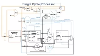
Datapath for a single-cycle MIPS implementation 0 M u x 1 Add PC 4 Add Shift left 2 PCSrc RegWrite MemToReg MemWrite Read address Instruction [31-0] I [25 - 21] Read register 1 Read data 1 ALU Read address Read data 1 M u x 0 I [20 - 16] Zero Read register 2 Instruction memory Read data 2 0 M u x 1 Result Write address 0 M u x 1 Write register Data memory Write data Registers I [15 - 11] ALUOp Write data MemRead ALUSrc RegDst I [15 - 0] Sign extend
Control • The control unit is responsible for setting all the control signals so that each instruction is executed properly • control unit’s input is the 32-bit instruction word • outputs are values for the blue control signals in the datapath • most signals can be generated from the instruction opcode alone • Our single-cycle implementation uses two separate memories, an ALU, some extra adders, and lots of multiplexers • On Friday, we’ll see the performance limitations of this single-cycle machine and discuss how to improve upon it