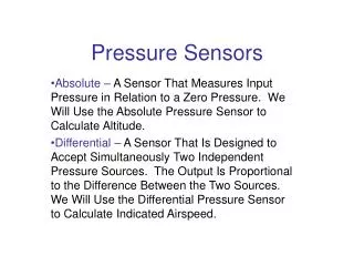
Absolute Pressure Sensors
Absolute Pressure Sensors. Z. Celik-Butler, D. Butler and M. Chitteboyina Nanotechnology Research and Teaching Facility University of Texas at Arlington http://www.uta.edu/engineering/nano/. Absolute Pressure Sensor Model in CoventorWare. Flexible superstrate. 0.14cm x 0.14cm.


Absolute Pressure Sensors
E N D
Presentation Transcript
Absolute Pressure Sensors Z. Celik-Butler, D. Butler and M. Chitteboyina Nanotechnology Research and Teaching Facility University of Texas at Arlington http://www.uta.edu/engineering/nano/
Absolute Pressure Sensor Model in CoventorWare Flexible superstrate 0.14cm x 0.14cm Sealed Pressure Sensor Wheatstone Bridge Configuration Cavity Stress, Strain and Displacement simulations for the pressure sensor is currently on-going Flexible substrate Bond Pads
Fabrication Process Flow for the Absolute Pressure Sensor Clean silicon wafer
Fabrication Process Flow for the Absolute Pressure Sensor 40 µm flexible polyimide substrate
Fabrication Process Flow for the Absolute Pressure Sensor Insulation layer 0.5 µm
Fabrication Process Flow for the Absolute Pressure Sensor Thick polyimide sacrificial layer 2.5 µm
Fabrication Process Flow for the Absolute Pressure Sensor Thin polyimide sacrificial layer 0.5 µm
Fabrication Process Flow for the Absolute Pressure Sensor Etch holes Membrane layer 1µm
Fabrication Process Flow for the Absolute Pressure Sensor Piezoresistors 0.5 µm
Fabrication Process Flow for the Absolute Pressure Sensor Aluminum metallization 0.5 µm
Fabrication Process Flow for the Absolute Pressure Sensor Bond pads Etch holes Encapsulant layer 0.5 µm
Fabrication Process Flow for the Absolute Pressure Sensor cross-section Cavity Release both the sacrificial layers Release both the sacrificial layers
Fabrication Process Flow for the Absolute Pressure Sensor Bond pads cross-section Cavity Deposit final sealing layer 0.6 µm
Fabrication Process Flow for the Absolute Pressure Sensor Bond pads Spin coat 40 µm flexible polyimide superstrate
Absolute Pressure Sensor ResultsSensor A (0.0 – 2.0 psi) DISPLACEMENT PLOT STRAIN XX PLOT STRAIN YY PLOT MISES STRESS PLOT
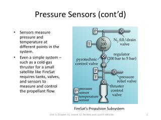
Absolute Pressure Sensor DesignSensor H (14.0 – 16.0 psi) DISPLACEMENT PLOT STRAIN XX PLOT STRAIN YY PLOT MISES STRESS PLOT
STEP 1 membrane layer ~ 0.1 µm • On a clean wafer spin-coat ~ 40 µm flexible polyimide as the substrate layer followed by 600 nm passivation layer STEP 2 Absolute Pressure Sensor Fabrication Steps • Spin coat thick polyimide and cure Piezoresistors ~ 25 nm STEP 3 • Spin coat thin polyimide and cure STEP 4 • Deposit 0.1 µm membrane layer STEP 5 • Deposit ~ 25 nm piezoresistor layer NEXT STEPS Passivation layer ~ 600 nm Thick Sacrificial layer ~ 7 µm Thin Sacrificial layer ~ 0.5 µm • Deposit ~ 500 nm thick aluminum as the metallization layer • Ash the sacrificial layer using oxygen plasma to suspend the membrane • Deposit 0.5 µm encapsulation layer followed by 0.5 µm as the final sealing layer • Etch the silicon wafer from the back side to get access to the bond pads and characterize the absolute pressure sensors
4 3 2 1 Absolute Pressure Sensor Characterization Vout Vin Vin Vout R3 R2 R4 R1 • The electrical circuit is complete with two active piezoresistors (R1 and R3) and two passive piezoresistors (R2 and R4) in a Wheatstone bridge configuration • The current-voltage characteristics is plotted and the true resistances are found • Pressure is applied on top of the membrane and the change in output voltage vs. input voltage is plotted