Download
1 / 40
430 likes | 746 Vues
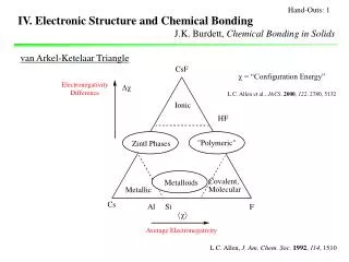
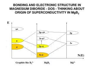
E. p*. 3 p -p*. 3p. 3s-*. p. 3s. 3 p -p. . 3s-. N(E). BONDING AND ELECTRONIC STRUCTURE IN MAGNESIUM DIBORIDE - DOS - THINKING ABOUT ORIGIN OF SUPERCONDUCTIVITY IN MgB 2. Graphite like B 2 2-. M g B 2. M g 2+.

E N D
E p* 3p-p* 3p 3s-* p 3s 3p-p 3s- N(E) BONDING AND ELECTRONIC STRUCTURE IN MAGNESIUM DIBORIDE - DOS - THINKING ABOUT ORIGIN OF SUPERCONDUCTIVITY IN MgB2 Graphite like B22- MgB2 Mg2+
SUPERCONDUCTIVITY IN MgB2 AT 39K A SENSATIONAL AND CURIOUS DISCOVERY • Metallic MgB2 known 1953, direct synthesis from Mg/B • Akimitsu Nature 2001, 410, 63 • Tc of 39K, surprising - Tc Nb3Ge 23K, LaxSr1-xCuO4 40K, YBa2Cu3O7 90K • Graphitic B22- sheets sandwiching hcc Mg2+ layers • Isoelectronic graphite is not a superconductor - only when doped at 5K? • Strong p-p bonding interactions between B6 rings and Mg • p-p stabilized wrt s-* of graphitic-like B22- sheets • Cooper pairs from excitation of p-p electrons into s-* • MgxAl1-xB2substitution extra electron fills s-* and reduces Tc • BCS Isotope effect of 1K on Tc for Mg10B2 higher than Mg11B2
Sealed quartz tube B/I2/Si/1100°C BI3/SiI4 VPT Tantalum tube MgO/5nm Au/B NWs/1000°C MgB2 NWs B NWs/Mg/800-900°C VPT AND VAPOR-LIQUID-SOLID (VLS) SYNTHESIS OF BORON NANOWIRES AND THEIR CONVERSION TO SUPERCONDUCTING MgB2 NANOWIRES
VPT AND VAPOR-LIQUID-SOLID (VLS) SYNTHESIS OF BORON NANOWIRES AND THEIR CONVERSION TO SUPERCONDUCTING MgB2 NANOWIRES Au dewetting on MgO on heating and cluster formation on MgO VLS growth of B NWs on Au clusters Au film on MgO
CONVERSION OF B NANOWIRES TO SUPERCONDUCTING MgB2 NANOWIRES MgB2 NWs on Au clusters B NWs on Au clusters Mg 800-900°
SYNTHESIS OF SUPERCONDUCTING MAGNESIUM BORIDE NANOWIRES • Planar hexagonal net of stacked B2- anionic layers with hexagonally ordered Mg2+ cations between the layers • VPT agent BI3/SiI4 • VLS growth of B NWs, diameter 50-400 nm, on controlled size Au/Si nanoclusters supported on MgO substrate • Vapor phase transformation of amorphous boron nanowires tocrystalline magnesium boride nanowires B MgB2
SUPERCONDUCTIVITY OF MAGNESIUM BORIDE NANOWIRES • Magnetization of MgB2 nanowires as a function of temperature under conditions of zero field cooling and field cooling at 100G • The existence of superconductivity within the sample is demonstrated by these measurements and the Meissner effect at ~ 33K • Potentially useful as building blocks in superconducting nanodevices and as low power dissipation interconnects in nanoscale electronics • Recently epitaxial thin films made for superconducting electronics ZFC Tc
RT ULTRAVIOLET ZnO NANOWIRE NANOLASERSVPT SYNTHESIS AND GROWTH
RT ULTRAVIOLET NANOWIRE NANOLASERSVPT SYNTHESIS AND GROWTHVPT carbothermal reductionZnO/C 905°C ===> ZnCO VPT ===> ZnO NW880°C
ZnO/C/905°C ZnCOVPT VPT AND VLS SYNTHESIS AND GROWTH OF ORIENTED ZnO NANOWIRES Sealed quartz tube reactor - fate of carbon deposited on glass VLS growth ZnO wires on 1-3.5 nm Aun on sapphire 880°C Alumina boat
VPT-VLS SYNTHESIS AND GROWTH OF ORIENTED ZnO NANOWIRES ZnO <0001> growth ZnCO C sapphire Aun
ZnO NW LASER 266 nm excitation 385 nm laser emission
RT ULTRAVIOLET NANOWIRE NANOLASERS • RT UV excitonic lasing action in ZnO nanowire arrays demonstrated • Self-organized <0001>oriented ZnO nanowires grown on 1-3.5 nm thick Au coated sapphire substrate, morphology related to fastest rate of growth of <0001> face • VPT carbothermal reduction ZnO/C 905°C ---> ZnCO ---> ZnO NW 880°C alumina boat, Ar flow, condensation process • Wide band-gap ZnO SC nanowires, faceted end and sapphire end reflectors, high RI ZnO cladded by lower RI air and sapphire, form natural laser cavities, diameters 20-150 nm, lengths up to 10 mm • QSEs yield substantial DOS at band edges and enhance radiative recombination due to carrier confinement • Under 266 nm optical excitation, surface-emitting lasing action observed at 385 nm with emission line width < 0.3 nm • The chemical flexibility and the one-dimensionality of these quantum confined nanowires make them ideal miniaturized laser light sources • UV nanolasers could have myriad applications, including optical computing, information storage, and microanalysis
RT ULTRAVIOLET NANOWIRE NANOLASERS • PXRD pattern of ZnO nanowires on a sapphire substrate • Only (000l) peaks observed, owing to well-oriented <0001> growth configuration • (A) PL emission spectra from nanowire arrays below (line a) and lasing emission above (line b and inset) the threshold, pump power for these spectra are 20, 100, and 150 kW/cm2 , respectively. • (B) Integrated emission intensity from nanowires as a function of optical pumping energy intensity • (C) Schematic illustration of a nanowire as a resonance cavity with two naturally faceted hexagonal end faces acting as reflecting mirrors • Stimulated emission from the nanowires was collected in the direction along the nanowire’s end-plane normal (the symmetric axis) • The 266-nm pump beam was focused to the nanowire array at an angle 10° to the end-plane normal, all experiments were carried out at RT
GaN NW LASER - TOPOGRAPHIC AND OPTICAL IMAGE OF UV LASING ACTION
VLS SYNTHESIS AND GROWTH OF ORIENTED GaN NANOWIRES Wurtzite type GaN <0001> growth Ga or Me3Ga/NH3/900°C sapphire Nin
individual GaN NW UV lasing action Lasing from ends lasing photoluminescence
TOPOTACTIC SOLID-STATE SYNTHESIS METHODS: HOST-GUEST INCLUSION CHEMISTRY • Ion-exchange, injection, intercalation type synthesis • Ways of modifying existing solid state structures while maintaining the integrity of the overall structure • Precursor structure • Open framework • Ready diffusion of guest atoms, ions, organic molecules, polymers, organometallics, coordination compounds into and out of the structure/crystals
TOPOTACTIC SOLID-STATE SYNTHESIS METHODS: HOST-GUEST INCLUSION CHEMISTRY • Penetration into interlamellar spaces: 2-D intercalation • Into 1-D channel voids: 1-D injection • Into cavity spaces: 3-D injection • Classic materials for this kind of topotactic chemistry • Zeolites, TiO2, WO3: channels, cavities • Graphite, TiS2, NbSe2, MoO3: interlayer spaces • Beta alumina: interlayer spaces, conduction planes • Polyacetylene, NbSe3: inter chain channel spaces
TOPOTACTIC SOLID-STATE SYNTHESIS METHODS: HOST-GUEST INCLUSION CHEMISTRY • Ion exchange, ion-electron injection, atom, molecule intercalation, achievable by non-aqueous, aqueous, gas phase, melt techniques • Chemical, electrochemical synthesis methods • This type of solid state chemistry creates new materials with novel properties, useful functions and wide ranging technologies
out of plane pp orbitals - p/p* delocalized bands sp2 in plane s bonding A VDW gap 3.35Å B C-C 1.41Å, BO 1.33 A ABAB stacked hexagonal graphite Pristine graphite - filled p band - empty p* band - narrow gap - semimetal GRAPHITE
GRAPHITE INTERCALATION COMPOUNDS 4x1/4 K = 1 8x1 C = 8 C8Kstoichiometry G (s) + K (melt or vapor) ® C8K (bronze) C8K (vacuum, heat) ® C24K ® C36K ® C48K ® C60K Staging, ordered guests, K to G charge transfer AAAA sheet stacking sequence K nesting between parallel eclipsed hexagons, Typical of many graphite H-G inclusion compounds
E C C8K electron transfer to C2pp CB - metallic C8Br electron depletion from C2pp VB - metallic p* p* CB p* E(F) Eg E(F) p p VB p N(E) GRAPHITE INTERCALATION ELECTRON DONORS AND ACCEPTORS SALCAOs of the p-pi-type create the p valence and p* conduction bands of graphite, very small band gap, essentially metallic conductivity properties in-plane 104 times that of out-of plane conductivity - thermal, electrical properties tuned by degree of CB band filling or VB emptying
TYPICAL INTERCALATION REACTIONS OF GRAPHITE • G (HF/F2/25oC) C3.3F to C40F • intercalation via HF2- not F- - less strongly interacting -more facile diffusion • G (HF/F2/450oC) CF0.68 to CF (white) • G (H2SO4 conc.) C24(HSO4).2H2SO4 + H2 • G (FeCl3 vapor) CnFeCl3 • G (Br2 vapor) C8Br
PROPERTIES OF INTERCALATED GRAPHITE • Structural planarity of layers often unaffected by intercalation - bending of layers has been observed - intercalation often reversible • Modification of thermal and electrical conductivity behavior by tuning the degree of p*-CB filling or p-VB emptying • Anisotropic properties of graphite intercalation systems usually observed - layer spacing varies with nature of the guest and the loading • CF: 6.6 Å, C4F: 5.5 Å, C8F: 5.4 Å
e Al contact SS contact Li anode CFx/C cathode Li+/PEO BUTTON CELLS LITHIUM-GRAPHITE FLUORIDE BATTERY
BUTTON CELLSLITHIUM-GRAPHITE FLUORIDE BATTERY • Cell electrochemistry • xLi + CFx xLiF + C • xLi xLi+ + e- • Cx+xF- + xLi+ + xe- C + xLiFNominal cell voltage 2.7 V • CFx safe storage of fluorine, intercalation of graphite by fluorine • Millions of batteries sold yearly, first commercial Li battery, Panasonic • Lightweight high energy density battery, just C/Li/F, cell requires SS anode/lithium anode/Li+ ion conductor/CFx-acetylene black/aluminum cathode
SYNTHESIS OF BORON AND NITROGEN GRAPHITES - INTRALAYER DOPING • New ways of modifying the properties of graphite • Instead of tuning the degree of CB/VB filling with electrons and holes using the traditional methods involve interlayer doping • Put B or N into the graphite layers, deficient and rich in carriers, enables intralayer doping with holes and electrons respectively • Also provides a new intercalation chemistry
SYNTHESIS OF AND BC3THEN PROVING IT IS SINGLE PHASE? • Traditional heat and beat • xB + yC (2350oC) BCx • Maximum 2.35 at % B incorporation in C • Poor quality not well-defined materials • New approach, soft chemistry, low T, flow reaction quartz tube • 2BCl3 + C6H6 (800oC) 2BC3 (lustrous film on walls) + 6HCl
CHEMICAL AND PHYSICAL CHARACTERIZATION OF BC3 • BC3 + 15/2F2 BF3 + 3CF4 • Fluorine burn technique • BF3 : CF4 = 1 : 3 • Shows BC3 composition • Electron and Powder X-Ray Diffraction Analysis • Shows graphite like interlayer reflections (00l)
CHEMICAL AND PHYSICAL CHARACTERIZATION OF BC3 • 2BC3 (polycryst) + 3Cl2 (300oC) 6C (amorph) + 2BCl3 • C (cryst graphite) + Cl2 (300oC) C (cryst graphite) • This neat experiment proves B is truly a "chemical" constituent of the graphite sheet and not an amorphous component of a "physical" mixture with graphite • Synthesis, analysis, structural findings all indicate a graphite like structure for BC3 with an ordered B, C arrangement in the layers
STRUCTURE OF BORON GRAPHITE BC3 4Cx1/4 + 2Cx1/2 + 10Cx1 = 12C 6Bx1/2 + 1Bx1 = 4B Probable layer atomic arrangement with stoichiometry BC3
CHEMICAL AND PHYSICAL CHARACTERIZATION OF BC3 • BC3 interlayer spacing similar to graphite • Also similar to graphite like BN made from thermolysis of borazine B3N3H6 • Four probe basal plane resistivity on BC3 flakes • s(BC3)AB ~ 1.1 s(G)AB, (greater than 2 x 10⁴ ohm-1cm-1)
L A I = V1/R1 Rsample = V2/I Rsample = (V2R1)/V1 r= Rsample (A/L) s = 1/r I V1 V2 Current Source R1 Ohmeter 4-PROBE CONDUCTIVITY MEASUREMENTS
REPRESENTATIVE BC3 INTERCALATION CHEMISTRY • BC3 + S2O6F2 (BC3)2SO3F Oxidative Intercalation • Note: O2FS-O--OSO2F, peroxydisulphuryl fluoride, weak peroxy-linkage, easily reduced to 2SO3F- • (BC3)2SO3F Ic = 8.1 Å, (C7)SO3F Ic = 7.73 Å, (BN)3SO3F Ic = 8.06 Å • BC3 Ic = 3-4 Å , C Ic = 3.35 Å, BN Ic = 3.33 Å • More Juicy intercalation chemistry for BC3 • BC3 + Na+Naphthalide-/THF (BC3)xNa (bronze, first stage, Ic ~ 4.3 Å) • BC3 + Br2(l) (BC3)15/4Br (deep blue)
ATTEMPT TO INCORPORATE NITROGEN INTO THE GRAPHITE SHEETS, EVIDENCE FOR C5N • Pyridine + Cl2 (800oC, flow, quartz tube) silvery deposit (PXRD Ic ~ 3.42 Å) • Fluorine burning of silver deposit CF4/NF3/N2 • No signs of HF, ClF1,3,5 in F2 burning reaction • Superior conductivity wrt graphite • Try to balance the fluorine burning reaction to give the nitrogen graphite stoichiometry of C5N - a challenge for your senses!!! 4C5N + 43F2 20CF4 + 2NF3 + N2
INTERCALATION SYNTHESIS OF TRANSITION METAL DICHALCOGENIDES • Group IV, V, VI MS2 and MSe2 Compounds • Layered structures • Most studied is TiS2 • hcp S2- • Ti4+ in Oh sites • Van der Waals gap
INTERCALATION SYNTHESIS OF TRANSITION METAL DICHALCOGENIDES • Li+ intercalated between the layers • Li+ resides in well-defined Td S4 interlayer sites • Electrons injected into Ti4+ t2g CB states • LixTiS2 with tunable band filling and unfilling • Localized xTi(III)-(1-x) Ti(IV) vs delocalized Ti(IV-x) electronic bonding models • VDW gap prized apart by 10%
SEEING INTERCALATION - DIRECT VISUALIZATION OPTICAL MICROSCOPY Intercalating lithium - see the layers spread apart