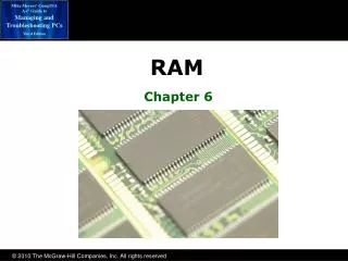
RAM
RAM. The level of satisfaction you have with your PC depends on the amount of RAM it has. Even if the processor is the fastest or the hard drive the best and quickest around, you just won’t get the performance you’re looking for without the right type and amount of

RAM
E N D
Presentation Transcript
RAM The level of satisfaction you have with your PC depends on the amount of RAM it has. Even if the processor is the fastest or the hard drive the best and quickest around, you just won’t get the performance you’re looking for without the right type and amount of RAM. So, it’s important for you to understand the various types of RAM starting from the earlier EDO to the current SDRAM and the future RDRAM. This will help you decide which RAM to buy for your PC.
Types of memory The following are the type memory that we are going to discuss in detail: ·Conventional memory ·Upper memory Area ·High Memory Area ·Extended Memory ·Expanded Memory ·Video RAM memory ·Adapter ROM and special purpose RAM ·Motherboard ROM BIOS Base or Conventional Memory DOS can read and write the entire mega byte, but can manage the loading of program only in the portion of first mega byte of RAM space called conventional Memory. Refer to figure 1. The 8088 processor and its equivalent will be able to address one megabytes of memory with 20-bit address lines. Out of one mega bytes of memory, 640 KB is used for DOS operating system and applications, and the remaining 384 KB is reserved for addressing BIOS ROM of motherboard, video adapter board, NIC card, video RAM and etc.
Upper Memory Area (UMA) The address space 384K above conventional memory is called Upper Memory Area. This memory has the addresses from A0000 through FFFFF. See figure 1. The first two 64 K blocks of UMA (address range from A0000-BFFFF) after conventional memory are reserved for video RAM. This space is used for storing video information like text and graphic data, in video RAM of Display Adapter before it is sent to the monitor screen. The next two 64 K blocks (address range from C0000-DFFFF) of UMA are reserved for the software programs, or adapter BIOS that is stored in ROM chip on the adapter plugged into the system slots. Most VGA compatible video adapters use the first 32 K Of this area for their onboard BIOS. The rest can be used for any other adapter plugged into the slots. The last two 64 K blocks (address range from E0000-FFFFF) of UMA are used for addressing the motherboard BIOS program stored in EPROM. This also contains POST (Power On self Test) bootstrap loader program, which initiate boot process from floppy or hard disk, CD-ROM drive and or from other drives. The last motherboard BIOS is allotted the address of 64 K (from E0000 – FFFFF). It is possible to load device drivers and memory resident programs in the unused space of UMA, which frees up the conventional memory otherwise they would occupy. The amount of free space available in UMA depends on the adapters plugged into Upper Memory Block (UMB).the system slots. The free space available in UMA is
Extended Memory The memory beyond first mega bytes that can be accessed through the protected mode of the 80286 and higher processors is generally called extended memory. Up to 16 Mega bytes of memory in 286 system and 4 Gigabytes in systems having processor 386 and above. Refer to figure.1 Only protected mode applications can use the extended memory in 286 machines. But with 386 and later microprocessors virtual 8086 mode allows software to split extended memory into one megabyte or smaller ranges that each act like base memory of an individual PC. Running several programs at the same time in virtual real mode, which is termed multitasking requires software that can manage each program from crashing into one another. Operating systems like Unix and Novell Netware, can directly access and load their OS Software into the extended memory. XMS Memory The Extended Memory Specification specifies how program would use the extended Memory. Several programs that use XMS memory can operate together under DOS on the same system, switching the processor into and out of protected mode to access the memory. XMS rules prevent one program from accessing memory that another program has in use. Extended memory can be made to conform the XMS specification by installing a device driver in the CONFIG.SYS file. The most common XMS driver is HIMEM.SYS Which is included with latest versions of DOS and Windows
High Memory Area (HMA) and the A 20 Lines The high memory area is an area of 64 K –16 bytes right on top of the first mega Bytes which can be accessed by 286 and higher processors in real mode whereas 8088 processor cannot access this area. In fact processors should not access beyond the first mega bytes in real mode. This is because processors (286 and above) having more than 20 address lines. This happens due to the (defect) bug present in these processors. That means when the segment and offset addresses are added together the resultant address spans the extended memory. The extended memory starts from 100000 (Hex). FFFF0 segment address FFFF offset address ---------- 10FFEF total ---------- If the 21st address line(A 20) of these processors is disabled these CPUs cannot access the HMA area. This can be done by using unused pins of 8042 keyboard controller on the motherboard to enable and disable A 20 address line with the help of HIMEM.SYS. Now the bug in these processors turned to be an advantage (feature) by using HMA area for loading DOS kernel in real mode. This is accomplished simply by first loading an XMS driver such as (HIMEM.SYS).
Expanded Memory Expanded memory is used to meet the demand of the applications, which require more memory space to run in PC and PC-XT. Expanded memory is located in an adapter board termed as Memory Expansion Board, which cannot be directly addressable, by processors like conventional memory and extended memory. Instead it can only be accessed through small 64 K window established in the unused area of the Upper Memory Area (usually from D0000-DFFFF). This segment (Window) is divided into 4 pages of 16 K each. When all the pages are filled one page is swapped into memory in memory expansion board, the page, which becomes empty can be used for loading required data for processing from the memory board. Using segment and offset concept, memory manager can address up to several megabytes in the memory board. Lotus, Intel and Microsoft developed driver program (LIM EMS) to exploit several mega bytes (32 MB) available in the card by the applications. It is only the way to run large applications, in systems using an 8088 processor. Only data can normally be placed in this segment because it is above the area of contiguous memory (640 K) that DOS can use. For example, a program cannot run while it is swapped out and therefore not visible by the processor.
ROM BIOS and MEMORY Conflicts If two adapters have overlapping ROM or RAM address, usually neither board operates properly. Each board functions if one removes or disable the other on, but they do not work together. With many adapters, one can change the actual memory location to be used with jumpers, switches, or driver software, which might be necessary to allow two boards to coexist in one system. Additionally one must ensure that adapter boards do not use the same IRQ (Interrupt Request Line), DMA channel (Direct Memory Access), or I/O Port address that lead to conflicts. ROM Shadowing In a high-end system reading ROM BIOS and adapter BIOS by either 8-bit or 16 bit at a time will bring down the performance (bottle neck) of the system. And also the speed of ROM available is very slow (150 to 200ns) comparing to System memory (DRAM/SDRAM with 60,40 ns or less). In 386 and higher systems, by moving the programming code from slow ROM chips into 32-bit system memory, processors can access the same code from system memory through 32 or 64 bit bus width and with speedier access. The shadowing is accomplished by using powerful Memory Management Unit in the 386 and higher processors. With appropriate instructions, the MMU can take a copy of the ROM code place it in RAM and enable the RAM chips that it appears to the system at exactly the same addresses where it was originally located. This actually disables the ROM chips, which are essentially shut down. The system RAM where ROM program resides is fully write protected.
Physical Memory Essential Memory Concepts the first step in any discussion of memory is to understand basically how memory works. If one as already has a good grasp of memory basics, feel free to skip this part of the chapter. Typical diagram of a Memory IC
Memory Types For a computer to work, the CPU must take program instructions and exchange data directly with memory. As a consequence, memory must keep pace with the CPU (or make the CPU wait for it to catch up). Now that processors are so incredibly fast (and getting faster), traditional memory architectures are being replaced by specialized memory devices that have been tailored to serve specific functions in the PC. As one upgrades and repair various systems, one will undoubtedly encounter some of the following memory designations DRAM (Dynamic Random-Access Memory) This remains the most recognized and common form of computer memory. DRAM achieves a good mix of speed and density, while being relatively simple and inexpensive to produce—only a single transistor and capacitor is needed to hold a bit. Unfortunately, DRAM contents must be refreshed every few milliseconds or the contents of each bit location will decay. DRAM performance is also limited because of relatively long access times. Today, many video boards are using DRAM SIMMs to supply video memory. SRAM (Static Random-Access Memory) The SRAM is also a classic memory design—it is even older than DRAM. SRAM does not require regular refresh operations, and can be made to operate at access speeds that are much faster than DRAM. However, SRAM uses six transistors (or more) to hold a single bit. This reduces the density of SRAM and increases power demands (which is why SRAM was never adopted for general PC use in the first place). Still, the high speed of SRAM has earned it a place as the PC’s L2 (or external) cache. One will probably encounter three types of SRAM cache schemes: asynchronous, synchronous burst, and pipeline burst.
Asynchronous Static RAM(Async SRAM or ASRAM) This is the traditional form of L2 cache, introduced with i386 systems. There is really nothing too special about ASRAM, except that its contents can be accessed much faster (20 ns, 15 ns, or 12 ns) than DRAM. ASRAM does not have enough performance to be accessed synchronously, and has long since been replaced by better types of cache. Synchronous-Burst Static RAM(Sync SRAM or SBSRAM) This is largely regarded as the best type of L2 cache for intermediate-speed motherboards (~60 to 66MHz). With access times of 8.5 ns and 12 ns, the SBSRAM can provide synchronous bursts of cache information in 2-1-1-1 cycles (i.e., 2 clock cycles for the first access, then 1 cycles per access—in time with the CPU clock). However, as motherboards pass 66MHz (i.e., 75 and 83MHz designs), SBSRAM loses its advantage to Pipelined Burst SRAM. Pipelined-Burst Static RAM (PB SRAM) At 4.5 to 8 ns, this is the fastest form of high performance cache now available for 75MHz+ motherboards. PBSRAM requires an extra clock cycle for “lead off,” but then can sync with the motherboard clock (with timing such as 3-1-1-1) across a wide range of motherboard frequencies. If one is interested in more technical details about PBSRAM, check out the ASUS site:
VRAM (Video Random-Access Memory) DRAM has been the traditional choice for video memory, but the ever-increasing demand for fast video information (i.e., high-resolution SVGA displays) requires a more efficient means of transferring data to and from video memory. Originally developed by Samsung Electronics, video RAM achieves speed improvements by using a “dual data bus” scheme. Ordinary RAM uses a single data bus—data enters or leaves the RAM through a single set of signals. Video RAM provides an “input” data bus and an “output” data bus. This allows data to be read from video RAM at the same time new information is being written to it. One should realize that the advantages of VRAM will only be realized on high-end video systems, such as 1024x 768 256 (or higher), where one can get up to 40% more performance than a DRAM video adapter. Below that, one will see no perceivable improvement with a VRAM video adapter. FPM DRAM (Fast-Page Mode DRAM) This is a popular twist on conventional DRAM. Typical DRAM access is accomplished in a fashion similar to reading from a book—a memory “page” is accessed first, then the contents of that “page” can be located. The problem is that every access requires the DRAM to re-locate the “page.” Fast-page mode operation overcomes this delay by allowing the CPU to access multiple pieces of data on the same “page” without having to “re-locate” the “page” every time—as long as the subsequent read or write cycle is on the previously located “page,” the FPDRAM can access the specific location on that “page” directly.
EDRAM (Enhanced DRAM) This is another, lesser-known variation of the classic DRAM developed by Ramtron International and United Memories. First demonstrated in August 1994, the EDRAM eliminates an external cache by placing a small amount of static RAM (cache) into each EDRAM device itself. In essence, the cache is distributed within the system RAM as more memory is added to the PC more cache is effectively added as well. The internal construction of an EDRAM allows it to act like page-mode memory—if a subsequent read requests data that is in the EDRAM’s cache (known as a hit), the data is made available in about 15 ns—roughly equal to the speed of a fair external cache. If the subsequent read requests data that is not in the cache (called a miss), the data is accessed from the DRAM portion of memory in about 35 ns, which is still much faster than ordinary DRAM. EDO RAM (Extended Data Output RAM) EDO RAM is a relatively well-established variation to DRAM, which extends the time that output data is valid—thus the word’s presence on the data bus is “extended.” This is accomplished by modifying the DRAM’s output buffer, which prolongs the time where read data is valid. The data will remain valid until a motherboard signal is received to release it. This eases timing constraints on the memory and allows a 15 to 30% improvement in memory performance with little real increase in cost. Because a new external signal is needed to operate EDO RAM, the motherboard must use a chipset designed to accommodate EDO. Intel’s Triton chipset was one of the first to support EDO. Although now most chipsets (and most current motherboards) currently support EDO. EDO RAM can be used in non-EDO motherboards, but there will be no performance improvement
BEDO (Burst Extended Data Output RAM) This powerful variation of EDO RAM reads data in a burst, which means that after a valid address has been provided, the next three data addresses can be read in only one clock cycle each. The CPU can read BEDO data in a 5-1-1-1 pattern (5 clock cycles for the first address, then one clock cycle for the next three addresses. Although BEDO offers an advantage over EDO, it is only supported currently by the VIA chipsets: 580VP, 590VP, 680VP. Also, BEDO seems to have difficulty supporting motherboards over 66MHz. SDRAM (Synchronous or Synchronized DRAM) Typical memory can only transfer data during certain portions of a clock cycle. The SDRAM modifies memory operation so that outputs can be valid at any point in the clock cycle. By itself, this is not really significant, but SDRAM also provides a “pipeline burst” mode that allows a second access to begin before the current access is complete. This “continuous” memory access offers effective access speeds as fast as 10 ns, and can transfer data at up to 100MB/s. SDRAM is becoming quite popular on current motherboard designs, and is supported by the Intel VX chipset, and VIA 580VP, 590VP, and 680VP chipsets. Like BEDO, SDRAM can transfer data in a 5-1-1-1 pattern, but it can support motherboard speeds up to 100MHz, which is ideal for the 75MHz and 82MHz motherboards now becoming so vital for Pentium II systems. Check out the following references for more information on SDRAM.
CDRAM (Cached DRAM) Like EDRAM, the CDRAM from Mitsubishi incorporates cache and DRAM on the same IC. This eliminates the need for an external (or L2) cache, and has the extra benefit of adding cache whenever RAM is added to the system. The difference is that CDRAM uses a “set-associative” cache approach that can be 15 to 20% more efficient than the EDRAM cache scheme. On the other hand, EDRAM appears to offer better overall performance. RDRAM (Rambus DRAM) Most of the memory alternatives so far have been variations of the same basic architecture. Rambus, Inc. (joint developers of EDRAM) has created a new memory architecture called the Rambus Channel. A CPU or specialized IC is used as the “master” device and the RDRAMs are used as “slave” devices. Data is then sent back and forth across the Rambus channel in 256-byte blocks. With a dual 250MHz clock, the Rambus Channel can transfer data based on the timing of both clocks—this results in data-transfer rates approaching 500MB/s (roughly equivalent to 2-ns access time). The problem with RDRAM is that a Rambus Channel would require an extensive re-design to the current PC memory architecture—a move that most PC makers strenuously resist. As a result, one is most likely to see RDRAM in high-end, specialized computing systems. Still, as memory struggles to match the microprocessor, PC makers might yet embrace the Rambus approach for commercial systems.
WRAM (Windows RAM) Samsung Electronics has recently introduced WRAM as a new video-specific memory device. WRAM uses multiple-bit arrays connected with an extensive internal bus and high-speed registers that can transfer data almost continuously. Other specialized registers support attributes, such as foreground color, background color, write-block control bits, and true-byte masking. Samsung claims data-transfer rates of up to 640MB/s—about 50% faster than VRAM—yet WRAM devices are cheaper than their VRAM counterparts. It is likely that WRAM will receive some serious consideration in the next few years.